Hello there,
after reading for months i decided to make my self finally an account, because now its time and i need ur support.
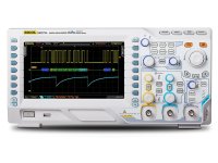
i am 22 years old, computer science student from germany. Until now i have always build either kits or subwoofers calculated with winisd. i have a umik1 for measuring
I am planning to build a 3 way floorstanding/ big standmount 3-way.
target specification:
-fully active
-should work without subs until 90dB(one preset with and one without sub)
i already bought/have:
subs:
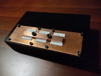
2x2 mivoc aw3000 in 40l cb impuls compensated with sure dsp, can produce 30-80Hz +-2dB at 100dB
new speaker:
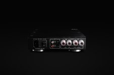
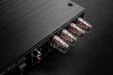
2xhypex fa123
2xkef sp1753 with flare
I am Planning to crossover at 350-400Hz and 2600-2900Hz
Woofer deaprtment should be smaller then 70l
Id like to stay below 28cm width and 40cm depth
I have yet not decided on woofer configuration, budget should not exceed 500€ for both speakers,
i thought about using subwoofers because i plan to cross quite low but i have never used subwoofers above 120Hz before is this a good idea?
1.
my first thought was to use 4x sb17nrx2c35-4 for each speaker to build somethink like a kef r11 but closed
~430€
Vituixcad(qtc=0,707, closed):
40l fb 69,9Hz
+headroom for eq
+with subwoofer should be possible to produce 110db >80Hz
-i dont user their mids at all(kind of a waste
😀)
1.1 same drivers but woofers impuls compensated like blade but in a floorstanding speaker with big baffle roundover at the front
+really like this idea
-i dont know if this approach even works in my room/ in general
-how do i simulate this kind of approach?
2.
use 2x dayton rs225-8
~380€
Vituixcad(qtc=0,707, closed):
44,3l fb 53,5Hz
+seems like a great performer
+good price
-i dont know if id like to look of it
3.
use 1 sb satori wo24p-8
~370€
Vituixcad(qtc=0,707, closed):
34,2l fb 46,4Hz
+seems like a very good driver
-bigger then everything else
-low max spl
-expensive
4.
maybe 2x visaton gf200in cb....
tiw200 a bit big but should work in a smaller box with eq / linkwitz transform
as u can read there is way to much posibilitys in woofer department and i cant deciede what to do and i find more woofers every day like wavecore, seas....
Can u tell me if my idea/plan with closed woofer is a good idea and which one u would chose?
Kef looks quite nice in room nearfield measurment and vituixcad with basic crossover between ht and mt