Clearly I must stand corrected regarding the relative availability of the 2SC4793 and 2SA1837. Since they are no longer being manufactured, I would still like to recommend the substitutions of TTC004B and TTA004B.
In the newer schematic, it seems that the cascode transistors M1 and M2 can be substituted for a wider variety of small Mosfets, perhaps even some from the ZVN series, such as ZVN2106A and ZVP2106A. M3 and M4 are handling the workload of driving the output stage.
In the newer schematic, it seems that the cascode transistors M1 and M2 can be substituted for a wider variety of small Mosfets, perhaps even some from the ZVN series, such as ZVN2106A and ZVP2106A. M3 and M4 are handling the workload of driving the output stage.
M1 and M2 of the folded cascode could also be BJTs, similar to those on the JFET drains. It would be nice if the output followers didn't need to be scarce Toshiba FETs.
...
In the newer schematic, it seems that the cascode transistors M1 and M2 can be substituted for a wider variety of small Mosfets, perhaps even some from the ZVN series, such as ZVN2106A and ZVP2106A. M3 and M4 are handling the workload of driving the output stage.
The max Vds of the ZVN2106A and ZVP2106A is 60V. That is a bit low for a +/- 28V swing (50W into 8R).
The ZVN3310A and ZVP3310A offer a higher voltage tradeoff.
Or the Toshiba BJT parts that I mentioned.
Or the Toshiba BJT parts that I mentioned.
Since they are no longer being manufactured
Follow the links and you may verify that those transistors ARE in current production by Unisonic in Taiwan. That does not preclude using the Toshiba devices. I just wanted to clarify that 2SC4793 and 2SA1837 are available and can be purchased from Profusion PLC in the U.K..
worth to mention - I'm completely happy with BD139/140, in most cases
my only wish could be to be able purchasing those with -16 suffix, (highest beta range), but there are so many more important things to solve 🙂
my only wish could be to be able purchasing those with -16 suffix, (highest beta range), but there are so many more important things to solve 🙂
the 2SC4793 and 2SA1837 don't seem to be available anywhere
It's a generic part, nothing special. I recently used some TIP31 and 32.
@Zen Mod
The high beta BD139 and BD140 are in stock at both Mouser and Digikey. Are you not able to find them in Europe?
The high beta BD139 and BD140 are in stock at both Mouser and Digikey. Are you not able to find them in Europe?
naah
I'm stumbling on them everywhere locally, so just lazy to search (order) for graded ones
when I need matched/graded ones (rarely), I just measure few and that's it
I'm stumbling on them everywhere locally, so just lazy to search (order) for graded ones
when I need matched/graded ones (rarely), I just measure few and that's it
It would be useful if we could find some SPICE models for the folded cascode FET and BJT alternatives. My suggested parameter requirements are:
- M1/M2 (2nd stage of folder cascode):
- Vds(Vce) >= 80V Watts >=1W
- M3/M4 source follower output stage:
- Vds >= 80V Watts >=3W
Just for fun, here are some models for the lateral Mosfets that I would try in place of M3/M4.
Also probably close enough for the old Hitachi parts and the newer Exicons.
.SUBCKT MSK1058 1 2 3
* TERMINALS: 1 2 3
M1 9 7 8 8 DMOS L=1U W=1U
RD 1 9 80.4M
RS 3 8 5.28M
RG 2 7 21.4
CGS 7 8 410P
EGD 12 0 7 9 1
VFB 14 0 0
FFB 9 7 VFB 1
CGD 13 14 128P
R1 13 0 1
D1 12 13 DLIM
DDG 15 14 DCGD
R2 12 15 1
D2 15 0 DLIM
DSD 8 1 DSUB
LS 30 3 7.5N
LD 1 9 4N
.MODEL DMOS NMOS (LEVEL=3 THETA=85M VMAX=163K ETA=2.2M VTO=.2 KP=.999)
.MODEL DCGD D (CJO=128P VJ=.6 M=.68)
.MODEL DSUB D (IS=29N N=1.5 RS=61.4M BV=160 CJO=802P VJ=.8 M=.42 TT=252N)
.MODEL DLIM D (IS=100U)
.ENDS
.SUBCKT MSJ162 1 2 3
* TERMINALS: 1 2 3
M1 9 7 8 8 DMOS L=1U W=1U
RD 9 1 110.4M
RS 8 3 25.28M
RG 7 2 17.4
CGS 7 8 760P
EGD 12 0 1 2 1
VFB 14 0 0
FFB 9 7 VFB 1
CGD 13 14 467P
R1 13 0 1
D1 12 13 DLIM
DDG 15 14 DCGD
R2 12 15 1
D2 15 0 DLIM
DSD 9 8 DSUB
LS 8 3 7.5N
LD 1 9 4N
.MODEL DMOS PMOS (LEVEL=3 THETA=90M VMAX=183K ETA=6.5M VTO=-.2 KP=1.109)
.MODEL DCGD D (CJO=467P VJ=.6 M=.68)
.MODEL DSUB D (IS=29N N=1.5 RS=61.4M BV=160 CJO=900P VJ=.8 M=.42 TT=252N)
.MODEL DLIM D (IS=100U)
.ENDS
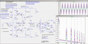
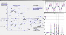
Pushing around equations today (no solder fumes) to better understand WHY the distortion cancellation circuit works. All of my previous analysis was of the 1st order small signal behavior which does not include any non-linear harmonic behavior. I do not know if my attempt at 2nd order behavior will succeed in discovering anything useful or not.
Maybe another candidate for the front-end ?
EUVL designed a headphone amplifier UTHAiM that can be configured for non global feedback, see "UTHAiM Public 170407 Part1.pdf" for detail.
EUVL designed a headphone amplifier UTHAiM that can be configured for non global feedback, see "UTHAiM Public 170407 Part1.pdf" for detail.
That does look like a good alternative FE. Every thing suggests that the FE be on a PCB separate from the OS its bias control circuits, allowing alternate FEs to be paired with the OS.
Indeed, much like:Every thing suggests that the FE be on a PCB separate from the OS its bias control circuits, allowing alternate FEs to be paired with the OS.
Attachments
- Home
- Amplifiers
- Pass Labs
- SIT measurements, Mu Follower, and amplifier build