Here are the main topics I intend to discuss:
- Sweet Spot Measurements of the Tokin 2SK182ES SIT.
- The SIT mu follower and its circuit relationships. I found some very simple equations describing the behavior of the mu follower.
- My build of an amplifier similar to the FirstWatt SIT-2.
Sweet Spot Measurements of the Tokin 2SK182ES SIT
The "Sweet Spot" is a circuit operating point where H2 (the 2nd harmonic distortion) is minimized, as described in http://www.firstwatt.com/pdf/art_sweet_spot.pdf. Later in this thread I will describe how understanding the sweet spot is important to the design of common source, single-ended and mu-follower amplifiers such as the Pass SIT-1 and SIT2.
In the next few postings I present some measurements of a single Tokin 2SK182ES SIT. I have made similar measurements of two other 2SK182ES SITs that currently reside in a stereo amplifier similar to the SIT-2 that delivers more than 20W/ch into 8 Ohms at about 2% THD into 8 Ohms. More about that amplifier later.
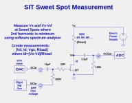
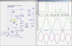
The first image below is a schematic showing the SIT in common source mode driving a resistive load Rload connected to a variable rail voltage Vx. The SIT gate is driven by an adjustable DC voltage from a signal generator, modulated by an AC sine signal from a DAC driven by a software spectrum analyzer. The AC voltage from the SIT drain is connected to the ADC input to the spectrum analyzer.
For a given resistor value Rload and rail voltage Vx, the DC voltage Vgs is manually adjusted to obtain a minimum value for H2, the 2nd harmonic. The DC voltage Vd of the SIT drain is measured. The drain current is calculated as Id=(Vx-Vd)/Rload. This operating point (Vd, Id, Vgs) is a 'sweet spot".
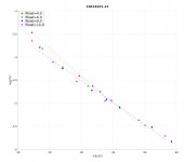
Here is a set of measurements with Rload = 8 Ohms.
Vd . . . . Id . . . Vgs
16.83 0.74500 -3.79
24.03 1.01625 -4.25
33.23 1.36250 -4.72
37.90 1.53375 -4.92
42.10 1.67750 -5.10
52.20 2.09375 -5.52
58.40 2.31375 -5.83
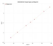
The second image is a plot of Id vs. Vds for these measurements at 8 Ohms. It is interesting to note that all of the sweet spots fall on a straight line in the Id vs. Vds plot.
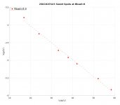
The third image is a plot of Vgs vs, Vds for these measurements, showing the same linear behavior.
The "Sweet Spot" is a circuit operating point where H2 (the 2nd harmonic distortion) is minimized, as described in http://www.firstwatt.com/pdf/art_sweet_spot.pdf. Later in this thread I will describe how understanding the sweet spot is important to the design of common source, single-ended and mu-follower amplifiers such as the Pass SIT-1 and SIT2.
In the next few postings I present some measurements of a single Tokin 2SK182ES SIT. I have made similar measurements of two other 2SK182ES SITs that currently reside in a stereo amplifier similar to the SIT-2 that delivers more than 20W/ch into 8 Ohms at about 2% THD into 8 Ohms. More about that amplifier later.
The first image below is a schematic showing the SIT in common source mode driving a resistive load Rload connected to a variable rail voltage Vx. The SIT gate is driven by an adjustable DC voltage from a signal generator, modulated by an AC sine signal from a DAC driven by a software spectrum analyzer. The AC voltage from the SIT drain is connected to the ADC input to the spectrum analyzer.
For a given resistor value Rload and rail voltage Vx, the DC voltage Vgs is manually adjusted to obtain a minimum value for H2, the 2nd harmonic. The DC voltage Vd of the SIT drain is measured. The drain current is calculated as Id=(Vx-Vd)/Rload. This operating point (Vd, Id, Vgs) is a 'sweet spot".
Here is a set of measurements with Rload = 8 Ohms.
Vd . . . . Id . . . Vgs
16.83 0.74500 -3.79
24.03 1.01625 -4.25
33.23 1.36250 -4.72
37.90 1.53375 -4.92
42.10 1.67750 -5.10
52.20 2.09375 -5.52
58.40 2.31375 -5.83
The second image is a plot of Id vs. Vds for these measurements at 8 Ohms. It is interesting to note that all of the sweet spots fall on a straight line in the Id vs. Vds plot.
The third image is a plot of Vgs vs, Vds for these measurements, showing the same linear behavior.
Attachments
Last edited:

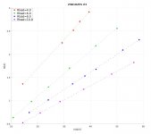
Similar sweet spot measurements were made with 4R, 6R, and 10R loads. The first image below shows Id vs. Vds plots of all the four data sets. Again the data falls on straight lines.
The second image shows Vgs vs. Vd plots of the four same data sets. It is very interesting that the Vgs vs. Vd curves fall nearly on top of each other. Given uncertainty about the FET junction temperature of each measurement, and instrumentation errors, is it possible that Vgs vs. Vd is independent of the Id and Rload?
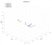
The third image shows a another view of the Id, Vds, Vgs space. (I haven't figured out a way to make the 3d plots available for adjustable viewing in the forum posts. Any suggestions would be appreciated).
The second image shows Vgs vs. Vd plots of the four same data sets. It is very interesting that the Vgs vs. Vd curves fall nearly on top of each other. Given uncertainty about the FET junction temperature of each measurement, and instrumentation errors, is it possible that Vgs vs. Vd is independent of the Id and Rload?
The third image shows a another view of the Id, Vds, Vgs space. (I haven't figured out a way to make the 3d plots available for adjustable viewing in the forum posts. Any suggestions would be appreciated).
Attachments
FrankenTracer measurements
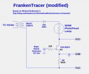
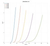
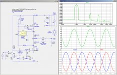
I also collected data using a varient of Michael Rothacher's FrankenTracer: Frankentracer Schematic | AudioMaker. The schematic of my test setup is shown in the first image, and the second image shows the Id vs. Vds curves for various Vgs values. The third image shows these plots combined with the sweet spot measurements.
In some following posts I will attempt to show the relevance of this data to the design of my amplifier.
Attachments
It is a pleasure to read your work. Inspiring as well.
I really like the IXYS depletion mode N-channel parts. I wish they offered them in a TO227 hockey puck. That package would be perfect for a Mu follower Tokin SIT build.
I am using the IXYS IXFN140N30P in the optocoupler based mu follower. No need for depletion mode.
SIT Sweet Spot Surface
I found the the sweet spot data for the form {Vd,Id,Rload} have a fairly simple equation
involving only 4 coefficients [A,B,C,D].
Id = A*Vd + B/Rload + C*Vd/Rload + D
This surface fit to the data plotted in post #4 is a twisted plane, as shown in the plots below. The mesh is rectangular grid in Id and Rload, with the height of the surface representing Id. The least-squares fit has a standard deviation of only about 25mA, which very good considering the instrumentation accuracy.
The equation above can be solve for Rload:
Rload=-(C*Vd + B) / (A*Vd - Id + D)
The significance of this result is that the parameters of the mu follower can chosen for a sweet spot at the desired idle state Vd and Id. More about this in later posts.
Attachments
Last edited:
Wow. I look at this and think "Wonder if a similar analysis would work with tube amplifiers?" Assign the control grid DC bias value with a function generator and move the tubes plate voltage (B+ voltage) value with another one. Try to find operating points with minimized harmonics along the line of constant quiescent power dissipation?
Replace the SIT with the triode in the schematic in post #2 and collect data triples: (Vp, Ip, Rload), where Vp it the plate voltage and Ip is the place current. I have no idea about the shape of the surface. Similarly, I have no data to suggest that all SITs behave as shown in post #10.
.......
The significance of this result is that the parameters of the mu follower can chosen for a sweet spot at the desired idle state Vd and Id. More about this in later posts.
This set of posts is so good it deserves a bump

yup

SIT Mu Follower Amplifier
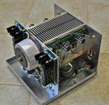
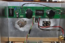
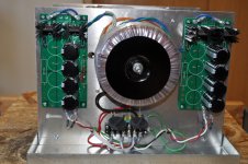
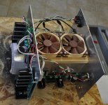
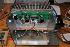
Here is the Common Source SIT Mu Follower amplifier that I have built, similar in topology to the FirstWatt SIT-2. The 2SK182ES SITs are capable of disipating considerable power. According to the datasheet, the package is rated at 500W dissipation, but the SOA is not specified. My inclination was to go for as much class-A power output as "reasonable", consistant with my favorite packaging approach which has the following characteristics:
Here is the Common Source SIT Mu Follower amplifier that I have built, similar in topology to the FirstWatt SIT-2. The 2SK182ES SITs are capable of disipating considerable power. According to the datasheet, the package is rated at 500W dissipation, but the SOA is not specified. My inclination was to go for as much class-A power output as "reasonable", consistant with my favorite packaging approach which has the following characteristics:
- Simple chassis fabrication. Only three metal parts (plus heatsinks).
- Heatsinks mounted fin-to-fin:
- 100W/chan passive
- >200W/chan with fans
- Easy board removal.
- Access for adjustments and scope probes.
Attachments
Last edited:
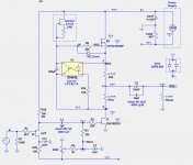
The amplifier topology is similar to that of the FirstWatt SIT-2, but uses an optocoupler instead of a simple transistor for controlling the bias current, and because of the high input capacitance of the 2SK182ES, a single-ended JFET buffer is added to drive the SIT gate. In the schematic shown below, the currents and node voltages are shown with a question mark (?), since many circuit parameters have not been yet specified.
Mu follower parameter adjustment:
The primary challenge was to determine the values for Rhi and Rmu. The sum Rhi+Rmu determines I0, the idle bias current of the two FETs. Rmu controls the mu-follower gain of the amplifier. Rmu=0 creates a constant current source. To simplify the experimentation with different values of Rhi and Rmu, I temporarily used a 20ga nichrome wire with 3 Molex connectors attached to nodes X, Y, and Z, as shown below. 20GA nichrome wire has a resistance of about 0.635 Ohms/ft. The connector at node Z can be adjusted to change the bias current without changing Rmu. Similarly, the connector mode Y can be used to change Rmu without changing the bias current. After changing the tap locations on the nichrome wire, the SIT gate bias is adjusted using the 500R pot to obtain the "sweet spot" using a 6R output load.
Attachments
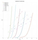
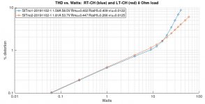
The 3rd figure shows a collection of sweeps of THD vs Watts sweeps of the for the left and right channels, respectively.
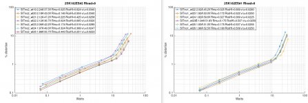
I experimented with many combinations of Rhi and Rmu. For each combination, the SIT bias voltage was adjusted to obtain the minimum 2nd harmonic H2 using a software spectrum analyzer. The voltage across the precision resistor Rsen in series with mu follower drain was used to deterimine the bias current Id0. The 500R potentiometer controls the gate voltage of the SIT which in turn controls the SIT drain voltage X0 (Vd0).
For each parameter combination THD was measured at Watt levels from less than .1 Watts to 30 Watts, as shown for the left and right channels in the images below. The parameters from those THD sweeps which give highest power output and lowest distortion are:
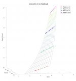
For my "final" build I removed the nichrome wires and installed fixed 3 Watt resistor combinations for Rmu and Rhi.
The 2nd figure shows the THD vs. Watts sweeps for the left and right channels with the fixed resistors.
I experimented with many combinations of Rhi and Rmu. For each combination, the SIT bias voltage was adjusted to obtain the minimum 2nd harmonic H2 using a software spectrum analyzer. The voltage across the precision resistor Rsen in series with mu follower drain was used to deterimine the bias current Id0. The 500R potentiometer controls the gate voltage of the SIT which in turn controls the SIT drain voltage X0 (Vd0).
For each parameter combination THD was measured at Watt levels from less than .1 Watts to 30 Watts, as shown for the left and right channels in the images below. The parameters from those THD sweeps which give highest power output and lowest distortion are:
- SITno2_wl25 left channel Id=1.88A Vd=55.7V Rmu=0R443 Rhi=0R251
- SITno1_wl24 right channel Id=1.82A Vd=59.6V Rmu=0R327 Rhi=0R369
For my "final" build I removed the nichrome wires and installed fixed 3 Watt resistor combinations for Rmu and Rhi.
- SITno2 left channel Id=1.81A Vd=53.7V Rmu=0R447 Rhi=0R266
- SITno1 right channel Id=1.59A Vd=58.5V Rmu=0R402 Rhi=0R409
The 2nd figure shows the THD vs. Watts sweeps for the left and right channels with the fixed resistors.
Attachments
- Home
- Amplifiers
- Pass Labs
- SIT measurements, Mu Follower, and amplifier build