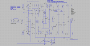
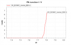
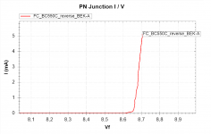
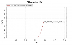
Here is a schematic with the Boxall transistors modified with Vbe reverse breakdown modeling. I never added this to models because there is not much data on it. But I would be satisfied with curve tracer results. Maybe ASTX can do some tests?
EDIT: wrong schematic.
EDIT: wrong schematic.
Attachments
Last edited:
I was told that a transistor degraded from reverse BE could be recovered using a forward BE current large enough to heat up the junction.
The SPICE models don't have reverse BE breakdown. The emitter with reverse voltage behaves something like a 5V zener diode, so once BVeb is exceeded the reverse current will be as high as the preceeding stage can sink.
On clipping the Veb of the Boxall drivers goes to 70V. In real life the BE junction would enter reverse breakdown.
A 1N4148 across the BC of the Boxall drivers would probably be enough to prevent degradation. This is pretty much the same as Logician's solution in his schematic. No penalty to THD.
With this I think it's more likely the Diamond follower will self-destruct before the Boxall drivers are degraded. So then the question is how often does this occur in the field?
Given what goes on inside an epitaxial reactor and ion implantation/diffusion furnace. I suppose anyone can get lucky at least once. But as the physics behind that suggestion are not presently clear to me I won't comment further.
How often does it occur in the field? Quite possibly every time it clips. How often does this lead to outright device failure in this particular application is another question entirely...
Also remember that whatever trans/diode may be used it will need a small eq cap to bootstrap into its junction.
My schematic also shows a simple fixed cascode used as an i/p stage current limiter.
This or something like would also have benefits against substantial shifts in operating point given the otherwise considerable and rapid thermal disturbances from clipping.
The only other frustrating thing about this i/p stage is that its not so readily servoable for DC operation.
Outside of that though I like it...
cheers, ian
The BC diodes , even with slight clip ... cause the whole Boxall/cascode to
conduct >30mA.Reverse bias is gone - <1V , but the HEAT of 30ma is there.
Which is worse ??
OS
I think it depends on the intent, do you want to protect against prolonged overdrive in serious abuse or do you just want to protect from rare mishaps like being plugged in while on, turning the source on while plugged in, static disharge etc.
When the VAS conducts 30mA it's Vce is likely small because the amplifier is clipping. The worst scenario would be dead short output where the VAS has high current and high Vce.
The VAS as long as it doesn't clip with high Ib or reverse Ib, will take some time to die. But a reverse Vbe event can degrade the amp permanently at the first mishap. I think that is why the issue is getting attention right now, other clipping faults have some abuse margin.
Last edited:
Here is a schematic with the Boxall transistors modified with Vbe reverse breakdown modeling. I never added this to models because there is not much data on it. But I would be satisfied with curve tracer results. Maybe ASTX can do some tests?
EDIT: wrong schematic.
And a clipping indicator , as well. Cool.
Will play with it.
Thanks , OS
I think it depends on the intent, do you want to protect against prolonged overdrive in serious abuse or do you just want to protect from rare mishaps like being plugged in while on, turning the source on while plugged in, static disharge etc.
When the VAS conducts 30mA it's Vce is likely small because the amplifier is clipping. The worst scenario would be dead short output where the VAS has high current and high Vce.
The VAS as long as it doesn't clip with high Ib or reverse Ib, will take some time to die. But a reverse Vbe event can degrade the amp permanently at the first mishap. I think that is why the issue is getting attention right now, other clipping faults have some abuse margin.
I was impressed by this IPS for how it handled a reasonable end-user
"overzealous" clipping event. I never simulated gross overload and never
considered the Boxall avalanche errata.
It would be nice to protect against both scenarios , I suppose it will come down to
a compromise between complexity/utility.
PS - some builders do not use the clamp diodes on DIYA's "badger". I have
not seen any fried badgers .... YET 😀.
OS
OS
People mostly copy what someone else has done.
TPC amps used to shunt to the rails, (I don't know who made the initial mistake).
Then Harry Dymond showed it was better to shunt to earth, and slowly the old circuits were replaced by better ones.
I suspect a similar case here, both in the way a poor decision was copied, and that it's better to shunt to earth.
I also expect that the difference is probably small - so there is not much pressure to find the better circuit.
But I think we may as well have the better one when there is no down side.
Of course, I could be mistaken, you could sim it and find out.
I may do it eventually, still at work on the compensation so I may not even need shunts.
But if I do I will check the idea.
Best wishes
David
Hi David,
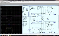
I normally use both - VAS output-to-ground and pre-drivers' (EF3) base-to-collector options. My logic is the following:
1) VAS output-to-ground is a good way of arranging the lag compensation in a CFA design. That one normally comes to 100pF-200pF (C19, C20 on the left picture).
2) Pre-drivers' base-to-collector capacitors are placed very close to those pre-drivers (behind their base stoppers if you look from the VAS side), in order to prevent possible local oscillation of EF3. 33pF-47pF on each side is enough here (C4, C5 on the right picture).
Cheers,
Valery
EDIT: added the pictures
Attachments


Last edited:
...I normally use both...
2) Pre-drivers' base-to-collector capacitors are placed very close to those pre-drivers (behind their base stoppers if you look from the VAS side), in order to prevent possible local oscillation of EF3...
Hi Valery.
That looks like a very fail-safe method because it will cope well with any PCB trace inductance and capacitance.
I must admit my recommendation did not consider such parasitics, so thank you for the reminder.
I would call such double security as "belt and braces", but your avatar shows neither.😉
Perhaps there is a different idiom in Russian?
Best wishes
David
Keantoken's idea is also a sensible solution, shunt to earth but decouple with a capacitor to the power rail as close as possible.
Last edited:
What about triple OPS CFA with active IPS load and IOTPC (output inclusive two pole compensation). I never built it, to many amps.😀
Best wishes OS with your green amp
Damir
Mine.
Attachments
Hi Valery.
That looks like a very fail-safe method because it will cope well with any PCB trace inductance and capacitance.
I must admit my recommendation did not consider such parasitics, so thank you for the reminder.
I would call such double security as "belt and braces", but your avatar shows neither.😉
Perhaps there is a different idiom in Russian?
Best wishes
David
Hi David,
It's not directly visible on the avatar picture, but I've got both main and reserve chutes in my backpack. The idea is exactly the same - if the "belt" fails - the "braces" are in place 😀 I used the reserve 4 times throughout my career.
Cheers,
Valery
1) VAS output-to-ground is a good way of arranging the lag compensation in a CFA design. That one normally comes to 100pF-200pF (C19, C20 on the left picture).
2) Pre-drivers' base-to-collector capacitors are placed very close to those pre-drivers (behind their base stoppers if you look from the VAS side), in order to prevent possible local oscillation of EF3. 33pF-47pF on each side is enough here (C4, C5 on the right picture).
I use RC at base-colector driver of EF3 and never failed. Sometime using C at pre-driver can hurt the sew rate. Slew rate is my first priority, second is harmonic profile.
Mine.
That looks pretty nice, and not so different to what I have arrived at.
I think Damir has provided an excellent foundation and now I just want to simplify it as much as possible.
I hope the compensation can be simplified but still keep the Two pole behaviour.
Best wishes
David
Last edited:
...I used the reserve 4 times...
I never used my reserve (my career was very short) but I know about redundancy in sky dive equipment.
It was just a joke of course, because the suit so obviously has no belt or braces.
Best wishes
David
It was just a joke of course
It was a good one 🙂
The Russian saying didn't come to my mind right away, but now I think I know one - it comes from some ancient times but I still find it very practical these days. The direct translation is somewhat difficult, but the idea is:
"The God saves the ones, who have the means in place for being saved." 😀
Cheers,
Valery
Have you built it?
Not, yet 🙂
First, I will build CFA with Latfet as output, of course it use OITPC compensation. It is request from my friend.
I think Damir has provided an excellent foundation and now I just want to simplify it as much as possible.
I hope the compensation can be simplified but still keep the Two pole behaviour.
David

I'm waiting...
People mostly copy what someone else has done.
TPC amps used to shunt to the rails, (I don't know who made the initial mistake).
Then Harry Dymond showed it was better to shunt to earth, and slowly the old circuits were replaced by better ones.
I suspect a similar case here, both in the way a poor decision was copied, and that it's better to shunt to earth.
I also expect that the difference is probably small - so there is not much pressure to find the better circuit.
But I think we may as well have the better one when there is no down side.
Of course, I could be mistaken, you could sim it and find out.
I may do it eventually, still at work on the compensation so I may not even need shunts.
But if I do I will check the idea.
Best wishes
David
I am a believer in the ground method , a couple more DB psrr ....
(below) boys at NAD , with the (present-2018) amp - they shunt
both ways.
What an interesting OPS with its nested FB's !!
OS
Attachments

blue led to the rescue ...
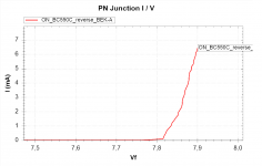
(below) reversed blue/uv led = only 3.2v reverse BE for the Boxall pair.
NO effect on normal (up to 2V input).
No effect at 2.2V , which is "enthusiastic" end user clipping.
A "screwup" , (5-10V input) causes 20-40mA pulses to pass through Q8/11 +
Q5/6 and the blue/uv leds.
$.66c X2 - https://www.mouser.com/datasheet/2/427/vlmu3100-211339.pdf
InGaN would most likely show less leakage short of Vf than the Nichia
GaN (old led) which I am simulating.
OS
Attachments
Voila - see attached images.Here is a schematic with the Boxall transistors modified with Vbe reverse breakdown modeling. I never added this to models because there is not much data on it. But I would be satisfied with curve tracer results. Maybe ASTX can do some tests?...
BR, Toni
Attachments
- Status
- Not open for further replies.
- Home
- Amplifiers
- Solid State
- GreenAmp ++ modulated Class G output