This seems to work pretty well. It reduces base recirculation at the problematic frequencies at the same time as it provides a constructive path for drive current for Q8, salvaging the most gain and bandwidth. Base recirculation of the cascode is not hindered either. I think this is close to optimal.
Attachments
This seems to work pretty well. It reduces base recirculation at the problematic frequencies at the same time as it provides a constructive path for drive current for Q8, salvaging the most gain and bandwidth. Base recirculation of the cascode is not hindered either. I think this is close to optimal.
Attack the SP directly !!
Works with the Bode , 39Mhz hump is gone. (below 1)
Lowers unity gain - no problem. More margin.
Will play with it.
OS
Attachments
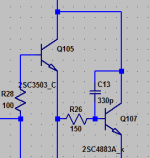
Original was direct lead compensation from the current FB.
Here I try a simple miller wrapped around the SP/cascode.
Same result.(below 1). No "hump" at 39Mhz.
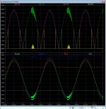
When excited by the schottky "glitches" , your method produced a less
damped result than now . Still , a hard clip affects the super-pair. At the
output , it still looks nice and rounded. (below 2)
Performance is the same , despite the bloody diodes. (below 3).
The CFA's speed absolutely outperforms any VFA in correcting class H
"errata".
OS
Here I try a simple miller wrapped around the SP/cascode.
Same result.(below 1). No "hump" at 39Mhz.
When excited by the schottky "glitches" , your method produced a less
damped result than now . Still , a hard clip affects the super-pair. At the
output , it still looks nice and rounded. (below 2)
Performance is the same , despite the bloody diodes. (below 3).
The CFA's speed absolutely outperforms any VFA in correcting class H
"errata".
OS
Attachments
Attachments
Ok, let’s investigate your design from the end.
First of, and maybe the main goal of amp’s design - is to create powerful but yet stable at all load conditions OPS.
I must let you know, that EF3 without special care are unstable at all. Symptomes are - you run the amp, set bias, all are first see similar to the sim.
But.
You feed the input with some kind of signal and all looks fine!
Being sure and delighted you load an amp to the test load and...
And all your OPS, including thick PCB traces and TO-247 devices, really flashes being destroyed in a single second. Even light bulb in series with mains can’t stop this, OPS capacitors energy are enough.
Refer to Colpitz generator for understanding reasons (just add lead and trace inductance in model), while there we’ll talk about possible resolving.
There are at least two known ways to eliminate this:
1. Build comparatively low-widebandness OPS, but without special testing and optimisation in each build sample referred to devices parameters scattering
2. Build comparatively high-frequency OPS, but each amp’s sample will need some specific tuning based on specific devices samples used.
Each ways are turning unstable EF3 to stable EF2 in specific HF region of unstability.
First way are simple - turn off first EF3 stage by RC circuit at the second stage bases. Just put ~100-220 Ohms in series and 120-470 pF paralleled to CB capacitance like i show in the previous post.
Second way are a little tricky. Use powerful fast drivers like KSA2690A (limits you to the +-60 V supply rails) with very slow output devices like MJL21194 or even BD911. Last ones have very high BE capacitance and drivers will blow their output current straightly to the load at HF. This approach demands relatively low OPS devices base stoppers in order of 2-3 Ohms and with BE capacitance they will form some kind of damper, this asks for some tuning based on driver samples fT which slightly varies.
While first approach are simpler it limits you in terms of usable bandpass, say 1-2 MHz of ULGF, second one will let you build an amp with unprecedently high ULGF at orders of 8-12 MHz. Stretching OPS passband will allow you to have much more feedback depth at 10-100 kHz region and allow your amp to eliminate OPS shoulders crossover effects, audible and known as “transistor sounding”.
Also, keep in mind, your load are reactive and electromechanic, so for example, put 4 TO-247 devices at 45 Volts rails are real necessity. You doesn’t need more output power for home use and i’ll prefer to build reliable powerful OPS at that rails instead of play with supply G- or H-class switching.
I really won't miss seeing the designs and performance details of one of your power amplifiers, can you please share them here!
Ok, let’s investigate your design from the end.
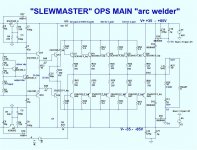
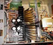
This EF3 is the "slewmaster". At least 500 built. Search for slewmaster.
I have one. No issues.
VZ audio (russia) uses similar output stages , no problems.
The only part of this design new is the class H outer device circuits.
the rest have been on hundreds of oscilloscopes and other testings.
OS
Ok, let’s investigate your design from the end.
First of, and maybe the main goal of amp’s design - is to create powerful but yet stable at all load conditions OPS.
I must let you know, that EF3 without special care are unstable at all. Symptomes are - you run the amp, set bias, all are first see similar to the sim.
But.
You feed the input with some kind of signal and all looks fine!
Being sure and delighted you load an amp to the test load and...
And all your OPS, including thick PCB traces and TO-247 devices, really flashes being destroyed in a single second. Even light bulb in series with mains can’t stop this, OPS capacitors energy are enough.
Refer to Colpitz generator for understanding reasons (just add lead and trace inductance in model), while there we’ll talk about possible resolving.
There are at least two known ways to eliminate this:
1. Build comparatively low-widebandness OPS, but without special testing and optimisation in each build sample referred to devices parameters scattering
2. Build comparatively high-frequency OPS, but each amp’s sample will need some specific tuning based on specific devices samples used.
Each ways are turning unstable EF3 to stable EF2 in specific HF region of unstability.
First way are simple - turn off first EF3 stage by RC circuit at the second stage bases. Just put ~100-220 Ohms in series and 120-470 pF paralleled to CB capacitance like i show in the previous post.
Second way are a little tricky. Use powerful fast drivers like KSA2690A (limits you to the +-60 V supply rails) with very slow output devices like MJL21194 or even BD911. Last ones have very high BE capacitance and drivers will blow their output current straightly to the load at HF. This approach demands relatively low OPS devices base stoppers in order of 2-3 Ohms and with BE capacitance they will form some kind of damper, this asks for some tuning based on driver samples fT which slightly varies.
While first approach are simpler it limits you in terms of usable bandpass, say 1-2 MHz of ULGF, second one will let you build an amp with unprecedently high ULGF at orders of 8-12 MHz. Stretching OPS passband will allow you to have much more feedback depth at 10-100 kHz region and allow your amp to eliminate OPS shoulders crossover effects, audible and known as “transistor sounding”.
Also, keep in mind, your load are reactive and electromechanic, so for example, put 4 TO-247 devices at 45 Volts rails are real necessity. You doesn’t need more output power for home use and i’ll prefer to build reliable powerful OPS at that rails instead of play with supply G- or H-class switching.
OK.
It's hard to do your #1 , we have fast devices.
We are kind of forced to do #2 , we use real fast pre-drivers and drivers >100Mhz ft ,
and isolate them with a R/C from the outputs .
This OPS (the EF3) is really similar to a Harmon Kardon 680 (below 1) ,
perhaps one of the more reliable and revered of HK integrated amps.
Here (below 2) is the one I have - the "slewmaster".
As far as class H reliability , this circuit is a based a CREST (pro amp) design .
These amps last 20 years in hard professional use. CREST rates only at 1Khz full power
with .1%THD . I have refined it to ...... (below 3).
I think I have them "WOOPED" bad !!! 1PPM 1K.
BTW , the oscillation was the super-pair - definitely. changing compensation
fully fixed it.
OS
Attachments
Last edited:
EF3 is sensitive for shure, but not impossible...
I use it with 3503/1381+4883/1859+6145/2223 configuration, and more than 50 was build in the last 2 years, without any problem, even I not use output coil...
But there was issue if I replaced the predriver with Toshiba TTC004b/TTA004b. There was a heavy oscillation, using highly capacitive speaker cable. This oscillation was killed the 5A fuse in the rails within few miliseconds, but finally the output devices survived. Replacing the predrivers back to any low current (Ic<100mA), and fast (Ft>150MHz) device, everything became perfect again.
Sajti
These amps last 20 years in hard professional use. CREST rates only at 1Khz full power
with .1%THD . I have refined it to ...... (below 3).
Was not too bad with -say- 500-600W output power. That amplifiers was developed to survive everything, but not to reach the best sound quality...
Sajti
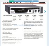
CREST CC1800
CREST PEAVEY CC1800 Service Manual download, schematics, eeprom, repair info for electronics experts
450W/8R !!
Greenamp is 1/2 the Crest. SO .. 200/350 should be it's 8/4R rating.
Greenamp X2 .. [later] will BE the Crest.
OS
CREST PEAVEY CC1800 Service Manual download, schematics, eeprom, repair info for electronics experts
450W/8R !!
Greenamp is 1/2 the Crest. SO .. 200/350 should be it's 8/4R rating.
Greenamp X2 .. [later] will BE the Crest.
OS
Attachments
Personally I like the old PRO version much more! I used them many times, and they are very reliable, as they use more output devices, comparing to the new series.
Sajti
Sajti
Do you want to see "greenamp X2" ?? COMING this spring !!Was not too bad with -say- 500-600W output power. That amplifiers was developed to survive everything, but not to reach the best sound quality...
Sajti
I'm on it now - OK , same 8 device total as the 1800. 100V rails.
And 400W at 3ppm. Got em' beat by X100 !!
OS
Attachments
Looks promising... I have some 800VA toroids, with 4x40V secondary 🙂
It would be fun to use them...
Sajti
It would be fun to use them...
Sajti
For maximum efficiency with music, the inner rail should be lower, ideally 25-30V, as discussed previously.
Looks promising... I have some 800VA toroids, with 4x40V secondary 🙂
It would be fun to use them...
Sajti
Check this out ....
Was not (entirely) the super- pair , after all.
OS
Attachments
Clip Safe?
My compliments to you for the careful work in this design and congrats on the latest spike reduction - an impressive result.
Have been looking at the headline question and can see how this would be an i/p stage well matched to the junction polarities of an EF/Beta enhancer arrangement with a good protection scheme or a stiff Baker clamp.
In the present design though there appear to be some clipping currents and potentials which, if I remember my old solid state physics correctly. Could irreversibly damage the emitter of the super pair input transistor?
Perhaps someone with a more complete or up to date knowledge of this phenomenon will contribute?
In my view; the abs max B/E reverse bias rating for that type of transistor i.e. 3~6V is probably best thought of as something along the lines of: OK; after passing a, probably less rather than more predictable, number of microamps at this value you could still have a working transistor. Sort of. But, if it were a bucket, it would probably be more useful as a collander.
As with collector base secondary breakdown. I seem to recall that a power transistor die may physically split due to highly localised lattice ionisation from quite small reverse e/b currents? Maybe some rad hard milspec stuff would just shrug it off?
Although less than conclusively informed I'd be inclined to limit reverse bias excursions of this junction to quite a small fraction of the abs max rating.
In the attached there are a few suggestions of quick and easy ways to minimise the prospect of any such damage.
However, these cheap and cheerful methods may impact thd and/or alter clipping waveform shape.
I hope these few thoughts are of use to you...
cheers, ian
Attachments
My compliments to you for the careful work in this design and congrats on the latest spike reduction - an impressive result.
Have been looking at the headline question and can see how this would be an i/p stage well matched to the junction polarities of an EF/Beta enhancer arrangement with a good protection scheme or a stiff Baker clamp.
In the present design though there appear to be some clipping currents and potentials which, if I remember my old solid state physics correctly. Could irreversibly damage the emitter of the super pair input transistor?
Perhaps someone with a more complete or up to date knowledge of this phenomenon will contribute?
In my view; the abs max B/E reverse bias rating for that type of transistor i.e. 3~6V is probably best thought of as something along the lines of: OK; after passing a, probably less rather than more predictable, number of microamps at this value you could still have a working transistor. Sort of. But, if it were a bucket, it would probably be more useful as a collander.
As with collector base secondary breakdown. I seem to recall that a power transistor die may physically split due to highly localised lattice ionisation from quite small reverse e/b currents? Maybe some rad hard milspec stuff would just shrug it off?
Although less than conclusively informed I'd be inclined to limit reverse bias excursions of this junction to quite a small fraction of the abs max rating.
In the attached there are a few suggestions of quick and easy ways to minimise the prospect of any such damage.
However, these cheap and cheerful methods may impact thd and/or alter clipping waveform shape.
I hope these few thoughts are of use to you...
cheers, ian
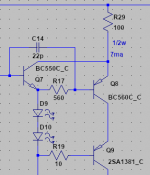
???? 😕
Where do you see the problem.
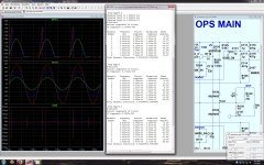
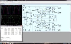
(below) is the Q7 and Q8 Ib and the total current through R18.
uA and native clamping from 7ma to 3ma on overload.
Edit - EF beta enhancer has slightly more gain but issues compared to the super pair .
Edit 2 - In the slewmaster thread , this IPS was built as the "kypton ND" , we ran it at clipping (overnight).
IPS VAS heatsink was cool in the morning (still clipping).
OS
Attachments

Last edited:
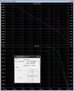
I see what you mean - Q7 reverse EB breakdown is approached at VERY
high overload.
But I noticed that Q7 emitter current falls to absolute Zero when this occurs.
The BC550C reverse V breakdown is 5V at 10 uA , we have 0 .
This is why it survives in real life.
What we have is a solution without a problem that becomes an ineffective solution
if the added diode leakage current is greater than the EB leakage current.
Still , this is far better than the beta enhanced EF phenomena.
OS
- Status
- Not open for further replies.
- Home
- Amplifiers
- Solid State
- GreenAmp ++ modulated Class G output