Vbe breakdown -
Reading ... yes , I do. 😀😀
I this case , we do not have the current available to do any damage (or make heat).
In fact , the avalanche (at <1uA) seem to be working in our favor.
OS
Reading ... yes , I do. 😀😀
Transistors have absolute maximum voltage spec's on their datasheets. The reverse-biased emitter-base junction is usually spec'd at 5V or 6V. A higher voltage , causes the junction to have avalanche breakdown (like a zener diode). The avalanche breakdown causes hot spots on the emitter-base junction and since it is not designed to dissipate heat like the collector is then the transistor is slowly damaged.
I this case , we do not have the current available to do any damage (or make heat).
In fact , the avalanche (at <1uA) seem to be working in our favor.
OS
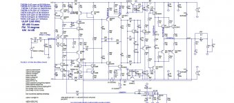
This EF3 is the "slewmaster". At least 500 built.
Ok. Let practice be truth criteria.
But "Slewmaster" have VAS loading resistance at an order of 680k, where are them now?
Removing them will raise the gain and allow you to achieve higher feedback depth.
But - what's the price?
I must let you know.
1. VAS output is a really current, not voltage as one could think by it's name. There are two high-output impedance current sources being loaded to each other.
VAS loading resistance converts "delta" of output current into output voltage and OPS, being voltage follower with high input impedance, must raise output current only.
2. Now you obsolete those resistance ('s), this will demand to convert VAS output current into voltage on OPS input impedance and current sources output impedance. Being really - all board parasitics, fingeroil, soldering mask leak, surface leak and etc. will both make a current path to the ground. Orders - some MOhm based on board material, manufacturing quality, soldering cleaning method, mounting touches at VAS output and etc.
All of this will provide you with unpredictable gain of the main gain stage, are you sure you need this in the first-order compensated amplifier?
Next.
Q9+Q10 bases must be grounded for AC signals while they arent.
There are three possible VAS outputs:
1. Clear common emitter, driven from base
2. Hybrid Vbe, driven from base AND emitter
3. Common base, driven from emitter only
First pair provides distortion by two effects, Miller and Early, while last one - only Early. While modern high-voltage trannies like 3503/1381 have very small Early effect why use CE or hybrid drive methods?
There are a best one from distortion perspective - CB and you doesn't need to use Baxandall/Shziklai pair to drive it.
That's the first see from the outside of the design team/
I'm sorry.
First order compensation with less than 40 dB feedback depth at 20 kHz?Search for slewmaster.
That's not the future i was learned to.
The impedance at the VAS output is limited by the 47pF capacitors at RF where it matters. Load resistors at the VAS output do nothing to improve measured performance. They make the forward gain variation worse, not better as is evidenced by the increased distortion.
That's the first see from the outside of the design team/
I'm sorry.
First order compensation with less than 40 dB feedback depth at 20 kHz?
That's not the future i was learned to.
Ok , I would like to see that 40db margin at 20K design.
As i see it 12db gets you single digit 20k ppm. If you want more ,
use error correction in the output stage.
The "outside design team" should submit proof !! 😀
OS
Ok. Let practice be truth criteria.
But "Slewmaster" have VAS loading resistance at an order of 680k, where are them now?
Removing them will raise the gain and allow you to achieve higher feedback depth.
But - what's the price?
Here I agree. About the same 20khz , but 30db more gain from there down.
These are gone , In fact I will recommend removing them from any
slewmaster IPS.
OS
OS, you should try two pole compensation, like TPC, TMC, or OITPC (Dadod) in CFA or Spooky amp (symmetry topology).
OS, you should try two pole compensation, like TPC, TMC, or OITPC (Dadod) in CFA or Spooky amp (symmetry topology).
Yes , I have tried it on this CFA super pair , it creates that 39mhz peak in
the middlebrook bode.
In the spooky , it works.
This brings me to a lot of advice that I have been given recently.
1. Bespav was right , any loading of the cascode VAS "wastes" gain.
## Corrected for this project and any slewmaster - since those 680k's were
(optional) anyways.
2. I respect the opinion of our long standing member Mr. Zan , but why do
NONE of the OEM's ground the predriver Ccb shunt ?? They ALL shunt to the rails.
3. Overload of the greenamp CFA. I have built /tested (as have others) ...
NO killing of this design - I do see that reverse BE issue , but only at 2X
clipping level (3+ volts).
Even here, the uA is not enough for heating (or punch-through) of the semi junction.
Worst case , with a 10V p-p preamp out overloading this amp , 20V reverse BE.
This might be bad ... but to what level do we make something "idiotproof".
My simulation of many OEM's shows even worse behavior on "gross" overload
- as do many of the present designs here at DIYA.
OS
What about triple OPS CFA with active IPS load and IOTPC (output inclusive two pole compensation). I never built it, to many amps.😀
Best wishes OS with your green amp
Damir
Best wishes OS with your green amp
Damir
Attachments

Last edited:
Rail switcher ?? Class G.
Just a position swap of the SiC diode and the omission of a few un-needed
components make for class G "rail-switcher".
I will add the (D-PAC SMD) pads on the OPS PCB to allow this.
I notice that in class G mode I get that 1K >.05% THD , just like the OEM's.
H is better , more SOA and efficiency.
I like this on a project , greenamp will accept any input stage AND
allow AB/H/or G. Fun for all !! This is how I layout the board.
PS - I could even make it LATERAL compatible ! I did this on the slewmaster
by allowing the predrivers to be omitted.
OS
Attachments
Last edited:
What about triple OPS CFA with active IPS load and IOTPC (output inclusive two pole compensation). I never built it, to many amps.😀
Best wishes OS with your green amp
Damir
Questions ??
1. Why , with 47pf shunts of the VAS/predrivers , do you need to also shunt the main drivers with 220pF (C15/16) ?
2. I LOVE Q33/Q34 , cascoding the "current pair".
3. With 5.6/6.8R degeneration, only at 2.65Mhz UG ?
Greenamp will be at 2.5Mhz with 22pf millers and 22 Re .
(33pF and 33Re is >2Mhz).
PS - notice the same redundant values in greenamp - easy sourcing !!
I still want to keep parts count down. I know transistors are cheap,
but builders will gravitate to simple designs. Why APEX has the most
builds. If I added IOTPC to the IPS/OPS , some would consider it
"complicated". An older class G/H thread here at DIYA discussed this
as a drawback to the technology. 🙁
OS
Last edited:
OS, you should try two pole compensation, like TPC, TMC, or OITPC (Dadod) in CFA or Spooky amp (symmetry topology).
Nowaday i’ll prefer to build very high gain amp, say at least 100-110 dB at 20 kHz, use 20 dB of that gain for input amplification and loop all remaining gain around amp’s core. All needed external compensation circuitry are well known for years, very simple to design and provides stable pole-zero positions (excluding output current floating OPS pole).
Anyway amplifier itself must be inverting or you need to have very-high CMRR and very low distortion input buffer.
Very high feedback depth with inverting connection will dither input signal with very much noise-cancelling feedback.
ULGF could be inside some MHz range by design, there are only two reliable nonswitching ways - EF3 and dynamical MOSFET cascode (SourceFollower1 with output tracking supply). Last one are very attractive to be bridged at +-40-55 supply rails - really high power without bipolars beta degradation effect at high output current, neglible input capacitance due to tracking and simple 2U OPS layout with TO-264’s.
It’s better to have as much as possible high-voltage low-current stages builded on common base topology.
Anyway you’ll need as low parasitic capacitance to mains as possible, i’ld prefer relatively high-freq half bridge with active PFC since we have remaining enough feedback depth at 100 kHz range, say evil and immortal 1ED Infineon drivers. At such powers mains trafo can’t be compact and low capacitance are preferred than some switching noise. Supply module could be build as external with huge capacitance distributed on the amp’s PCB’s.
Classical G/H amps can prepare for their own funeral managed by modern TD ones.
Questions ??
1. Why , with 47pf shunts of the VAS/predrivers , do you need to also shunt the main drivers with 220pF (C15/16) ?
2. I LOVE Q33/Q34 , cascoding the "current pair".
3. With 5.6/6.8R degeneration, only at 2.65Mhz UG ?
Greenamp will be at 2.5Mhz with 22pf millers and 22 Re .
(33pF and 33Re is >2Mhz).
PS - notice the same redundant values in greenamp - easy sourcing !!
I still want to keep parts count down. I know transistors are cheap,
but builders will gravitate to simple designs. Why APEX has the most
builds. If I added IOTPC to the IPS/OPS , some would consider it
"complicated". An older class G/H thread here at DIYA discussed this
as a drawback to the technology. 🙁
OS
1. You are right, it's better to shunt predrivers than drivers, this is old schematic and I do now like that.
3. ULGF is not so easy to calculate, this is complicate compensation and I optimized it by simulation. The Bode plot slop is 20dB/decade.
You can look for OITPC explanation in dedicated thread OITPC - Output inclusive TPC (not TMC)
BR Damir
2. I respect the opinion of our long standing member Mr. Zan , but why do
NONE of the OEM's ground the predriver Ccb shunt ?? They ALL shunt to the rails.
Possibly because with RC filters for the frontend rails, there was no significant improvement in distortion (depending on the specific design). I think the best way to handle this would be to have decoupling capacitors right at the predriver collectors, and move the 47pF caps to the ground side of the decoupling. That way you don't increase the loop distance between the base and collector through the capacitors. But unless there is a real benefit, save your energy for things that do matter.
Cross purposes?
Hi OS thank you for your courteous, well considered and dilligent response. Much appreciated.
Firstly, the image covers base emitter currents only beyond the 6 volt abs max threshold. I can't recall the proper smooth function but it is likely non linear and in all probability very individual device specific. So 10ua at 6 volts could well be far lower at 10v and even lower again for the next sample.
Secondly, a brief caveat about data sheets. Where; what you read, can be much less important than what wasn't included.
Thirdly, just a comment from memory which, as I am looking back to over 40 years ago, may now well be failing with age.
There are probably at least two major phenomenon to consider. The first is, as above, at the junction.
The other is in the central region of the emitter land(s) where these really very small currents can get damagingly intense. With increasing e-field strength, charge becomes localised to tiny groups of just a few atoms where it is then sufficiently concentrated to cause one lattice disruption after another and so on. This can happen not only from implantation/diffusion irregularities but also through clean room/process contaminants.
These and some other causes can leave the device still operational. But only around the periphery of its emitter. In all likelyhood, after this, some aspects of its performance may be at best marginal against its original condition.
Unless memory fails, back then in the dark ages, the chief culprit for this 'pepperpotting' was eventually identified as Iron. But it will, in any event of these bias conditions, still happen due to ordinary lattice field variations.
My take away from all this is:
Down at that scale; its much more to do with the voltages than currents; of which, any are probably enough to do some damage.
Finally though, a happy conclusion, because I can't imagine a better job for a transistor that could well have endured such treatment than the light duties of first in a super pair.
Good luck and success with the project.
cheers, ian
I see what you mean - Q7 reverse EB breakdown is approached at VERY
high overload.
But I noticed that Q7 emitter current falls to absolute Zero when this occurs.
The BC550C reverse V breakdown is 5V at 10 uA , we have 0 .
This is why it survives in real life.
What we have is a solution without a problem that becomes an ineffective solution
if the added diode leakage current is greater than the EB leakage current.
Still , this is far better than the beta enhanced EF phenomena.
OS
Hi OS thank you for your courteous, well considered and dilligent response. Much appreciated.
Firstly, the image covers base emitter currents only beyond the 6 volt abs max threshold. I can't recall the proper smooth function but it is likely non linear and in all probability very individual device specific. So 10ua at 6 volts could well be far lower at 10v and even lower again for the next sample.
Secondly, a brief caveat about data sheets. Where; what you read, can be much less important than what wasn't included.
Thirdly, just a comment from memory which, as I am looking back to over 40 years ago, may now well be failing with age.
There are probably at least two major phenomenon to consider. The first is, as above, at the junction.
The other is in the central region of the emitter land(s) where these really very small currents can get damagingly intense. With increasing e-field strength, charge becomes localised to tiny groups of just a few atoms where it is then sufficiently concentrated to cause one lattice disruption after another and so on. This can happen not only from implantation/diffusion irregularities but also through clean room/process contaminants.
These and some other causes can leave the device still operational. But only around the periphery of its emitter. In all likelyhood, after this, some aspects of its performance may be at best marginal against its original condition.
Unless memory fails, back then in the dark ages, the chief culprit for this 'pepperpotting' was eventually identified as Iron. But it will, in any event of these bias conditions, still happen due to ordinary lattice field variations.
My take away from all this is:
Down at that scale; its much more to do with the voltages than currents; of which, any are probably enough to do some damage.
Finally though, a happy conclusion, because I can't imagine a better job for a transistor that could well have endured such treatment than the light duties of first in a super pair.
Good luck and success with the project.
cheers, ian
Attachments

Last edited:
I was told that a transistor degraded from reverse BE could be recovered using a forward BE current large enough to heat up the junction.
The SPICE models don't have reverse BE breakdown. The emitter with reverse voltage behaves something like a 5V zener diode, so once BVeb is exceeded the reverse current will be as high as the preceeding stage can sink.
On clipping the Veb of the Boxall drivers goes to 70V. In real life the BE junction would enter reverse breakdown.
A 1N4148 across the BC of the Boxall drivers would probably be enough to prevent degradation. This is pretty much the same as Logician's solution in his schematic. No penalty to THD.
With this I think it's more likely the Diamond follower will self-destruct before the Boxall drivers are degraded. So then the question is how often does this occur in the field?
Attachments
Last edited:
1 - Nowaday i’ll prefer to build very high gain amp, say at least 100-110 dB at 20 kHz, use 20 dB of that gain for input amplification and loop all remaining gain around amp’s core. All needed external compensation circuitry are well known for years, very simple to design and provides stable pole-zero positions (excluding output current floating OPS pole).
Anyway amplifier itself must be inverting or you need to have very-high CMRR and very low distortion input buffer.
Very high feedback depth with inverting connection will dither input signal with very much noise-cancelling feedback.
ULGF could be inside some MHz range by design, there are only two reliable nonswitching ways - EF3 and dynamical MOSFET cascode (SourceFollower1 with output tracking supply). Last one are very attractive to be bridged at +-40-55 supply rails - really high power without bipolars beta degradation effect at high output current, neglible input capacitance due to tracking and simple 2U OPS layout with TO-264’s.
It’s better to have as much as possible high-voltage low-current stages builded on common base topology.
Anyway you’ll need as low parasitic capacitance to mains as possible, i’ld prefer relatively high-freq half bridge with active PFC since we have remaining enough feedback depth at 100 kHz range, say evil and immortal 1ED Infineon drivers. At such powers mains trafo can’t be compact and low capacitance are preferred than some switching noise. Supply module could be build as external with huge capacitance distributed on the amp’s PCB’s.
2 -Classical G/H amps can prepare for their own funeral managed by modern TD ones.
#1 - SHOW the design !!
#2 - Well , lets give class G/H one hell of a "funeral party" with the greenamp.
OS
I was told that a transistor degraded from reverse BE could be recovered using a forward BE current large enough to heat up the junction.
The SPICE models don't have reverse BE breakdown. The emitter with reverse voltage behaves something like a 5V zener diode, so once BVeb is exceeded the reverse current will be as high as the preceeding stage can sink.
On clipping the Veb of the Boxall drivers goes to 70V. In real life the BE junction would enter reverse breakdown.
A 1N4148 across the BC of the Boxall drivers would probably be enough to prevent degradation. This is pretty much the same as Logician's solution in his schematic. No penalty to THD.
With this I think it's more likely the Diamond follower will self-destruct before the Boxall drivers are degraded. So then the question is how often does this occur in the field?
So , no avalanche in the models.
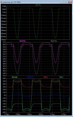
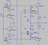
A way around this is to "jury rig" a reverse 4.7V zener to see. OOh , 65ma @ 4V global input.. Not good. (below - D15 is the zener).
Keen , show (the "Boxall" - you got it right !) which BC (Q7-8)?
Might we limit the input to the diamond ? This effect does not occur until
input is >3V (6Vp-p) ?
PS - "in the field" , they are more likely to place a wrong servo op-amp or
use EBC instead of BCE when assembling. Or , reverse a zener. I have
seen it all , but they have not exploded into fire. Maybe a OPS stuck to a rail ! 😀
Edit - I see , Keen. Was not logged on.
OS
Attachments
Last edited:
...why do NONE of the OEM's ground the predriver Ccb shunt ?? They ALL shunt to the rails.
People mostly copy what someone else has done.
TPC amps used to shunt to the rails, (I don't know who made the initial mistake).
Then Harry Dymond showed it was better to shunt to earth, and slowly the old circuits were replaced by better ones.
I suspect a similar case here, both in the way a poor decision was copied, and that it's better to shunt to earth.
I also expect that the difference is probably small - so there is not much pressure to find the better circuit.
But I think we may as well have the better one when there is no down side.
Of course, I could be mistaken, you could sim it and find out.
I may do it eventually, still at work on the compensation so I may not even need shunts.
But if I do I will check the idea.
Best wishes
David
Last edited:
The BC diodes , even with slight clip ... cause the whole Boxall/cascode to
conduct >30mA.Reverse bias is gone - <1V , but the HEAT of 30ma is there.
Which is worse ??
OS
conduct >30mA.Reverse bias is gone - <1V , but the HEAT of 30ma is there.
Which is worse ??
OS
I like to call it Boxall because it is unlikely to be confused with another circuit.
https://www.diyaudio.com/forums/solid-state/235695-nfb-line-amp-gainwire-mk2-67.html#post4259610
Some LEDs can be used to limit Diamond current. Of course once you start looking for clipping faults, you find them everywhere. The LEDs need a series diode to prevent them from going into reverse breakdown (maybe this is okay if they are more durable than BJTs). The Diamond drivers need B-E protection diodes as well, because when the LEDs start conducting the drivers then become reverse BE driven.
Attachments
- Status
- Not open for further replies.
- Home
- Amplifiers
- Solid State
- GreenAmp ++ modulated Class G output