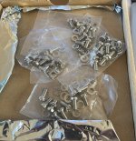
Nelson Pass testing procedure and instructions for DIY Sony Vfet amp -
Print this out!!
🙂
http://www.firstwatt.com/pdf/art_diy_sony_vfet.pdf
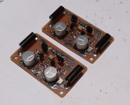
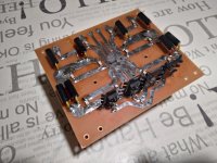
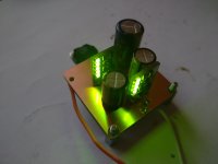
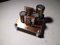
Pass DIY Sony Vfet amplifier illustrated build guide.
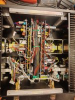
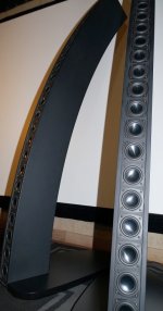
The Pass DIY Sony Vfet is a power amplifier from the brilliant mind of our technical, spiritual, and menu advisor, Nelson Pass. Quite possibly the most generous design yet, as Nelson released his private stash of the out of production 1970's Vfet to the DIY community so we can build an amp that nobody else can build nor buy.
🙂
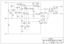
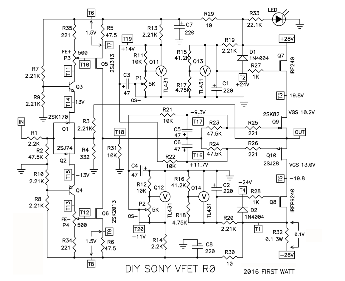
How the circuit works
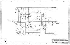
The Front End
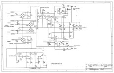
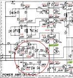
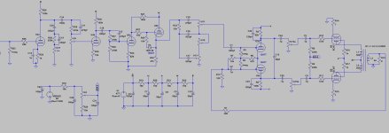
The overall schematic of the VFET amp is somewhat complicated in spite of the simple gain path – this is due to the special DC regulation circuits to cater to the fussy VFET transistors in the output stage.
Fortunately the front end voltage gain stage of the amplifier is pretty simple.
The Vfet DIY Front-end is basically a mini-F5. It serves to give us enough voltage and current gain to drive the Vfets so we can wire the Vfet as followers (known as “Common Drain operation, where no voltage gain is acquired, only current).
The input signal starts at R1 (2,2K), which acts as a “gate-stopper” resistor for the input Jfets, as well as a current limiter in case the attached preamp has a big turn-on or -off thump. R2, (47K) is from the input of the Jfet to ground, this gives the Jfet gates a reference to ground, and also sets the input impedance, which is about 50K.
The signal goes through the Jfets (Q1,2) and the gain currents at their Drain outputs go through the cascode transistors (Q3,4) and then to drive the Gates of the voltage amplification (Vas) Mosfets (Q5,6). The cascode transistors, Q3 and Q4, act as a voltage umbrellas, protecting the Jfets from the voltages appearing at T11 and T13 so that their Drains experience a fraction of the DC and AC voltage T11 and T13 as determined by R7, R9 and R8, R10 driving Q3 and Q4.
To quote Mr. Pass, “Cascoding is a very useful technique where the gain transistor (in this case each of the Jfets) is coupled to another transistor operated in Common-Gate or Common-Base mode. This cascode transistor contributes very little of its own characteristic to the amplification, but it acts like a voltage umbrella, shielding the gain transistor from the high DC voltage and noise of the power supply rails.”
The Drain pins of Q5 and Q6 deliver the output voltage (but not enough current) to drive loudspeakers. This point is found at test node T18.
Mosfet Q5 and Q6 need some voltage applied to their gates in order to turn on (bias) and amplify signal, and this is provided by the voltage appearing across R35 + P3 and R34 +P4. P3 and P4 are there to adjust this voltage so as to set the right amount of current through Q4 and Q6. This right amount of current is defined by 1.5 V DC appearing across resistors R5 and R6 AND the output of the front end (T18) near 0 volts DC. So P3 and P4 not only adjust the idle current through the voltage gain transistors Q5 and Q6, but they also set the DC output that appears on their Drain pins.
Adjusting the Front End bias
Bias is set by measuring the DC voltage across R5, (test nodes T6-T7), and R6 (test nodes T8-T9). Proper bias is when you have 1.5V across each of these resistors, at the same time also having 0 volts DC offset, which is the voltage at T18 to GND.
Adjusting P3 and P4 will make changes in all three of those readings, so in my opinion, you must have three DC voltmeters to make this an easy job. Even the very inexpensive Chinese DMM will work fine for this, just make sure they have good, fresh batteries in them.
A single voltmeter will do that job, but it is more tedious. In any case you want to adjust each pot in small steps, going between the pots and voltage measurements in rotation.
You start with both potentiometers at full counterclockwise, which is the lowest bias setting. At first you are simply looking to get the voltages across R5 and R6 up to 1.5 in small steps. You turn P3 just a little bit, measuring a small change across R5, and then you do the same for P4 and R6. And then you go back to P3/R6 and repeat this process, raising the DC voltages slowly and in equal amounts.
You also want to check the DC voltage from T18 to ground as you do this – you want to keep it near 0V if possible.
I suggest you pause at around 1 V on R5 and R6 – as the Mosfets heat up, the current will rise on its own. Eventually you will find yourself with “warm” settings which give about 1.5V DC bias and close to 0 V DC output at T18.
How good is good enough? 1.3 V to 1.7V is OK for bias. +/-200 mV is good enough for offset at this point. We will tweak these values after the completed amplifier has run for a bit.
REMEMBER – BABY STEPS ON ALL ADJUSTMENTS.
If for some reason you can’t achieve full bias with zero offset, please troubleshoot in the build guide thread, and do tell us how much bias you can get with zero offset.
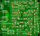
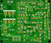
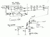
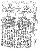
Please refer to the above schematic for component names
The output stage -
The Vfets themselves are wired as a complementary pair in source-follower mode. These add current gain to the signal sent to their Gate pins (to be able to drive speakers with a low output impedance) but have no voltage gain.
That’s it - the voltage gain has happened in the Front-End, and the Vfets just add current capability.
🙂
But it’s not quite that simple… is it?
Well, it actually is, until you realize that the DC powering up the Vfets must be regulated for a stable DC voltage and low noise, the same with the bias voltage. Also, both the rail voltage and the bias voltage have to power-up and power-down in a specific order to keep the Vfets from trying to draw a ton of current when the circuit is powered up.
What’s the proof of Nelson’s genius in this circuit? In how simple (and quite effective) the regulator sections have been designed. Let’s talk about that now.
Regulators
Each rail of each channel has 2 regulators, for a total of 4. Each of the two rails has a bias regulator and an output stage regulator. For clarity’s sake, I’m now going to talk about the positive rail’s regs - the negative rails have the same thing, just in a mirror image.
Both regulators use a TL431, a nice little 3-pin shunt reg that can have it’s output voltage set by 2 resistors.
Looking at the schematic around Q11, you can see the unregulated voltage coming from the rail through a simple RC filter (R29 and C7) then through R13 (2.21K) and then the set resistors R11 (10K) and P1 (5K pot).
Because one of the two set resistors is a potentiometer wired as a variable resistor, changing that pot value changes the set voltage which provides Vfet voltage bias.
It is very important that the bias voltage is place when power is applied to the Drain of the VFET, so this regulator circuit (bias reg) is designed to charge up much faster than the regulated voltage powering the Drain. (The output stage regulator)
Remember how it was mentioned earlier that the Sony Vfets are “Depletion” mode? They are normally on, letting current flow, and require a negative voltage applied to the gate to turn them off (this for the N type – The P channel devices require a positive voltage), or to otherwise set the value of the current (bias) through the VFET.
Looking at the regulated voltage at T19, (+14V) you want to note that it crosses over and connects to the gate of the negative P-channel Vfet Q10. The positive N-channel Vfet Q9, is likewise biased from the opposite rail. This is the opposite of what you are normally going to see with complementary Mosfet followers.
Moving on to the output regulators, you can see the circuitry near Q13 looks similar to the other reg, the exception being the voltage setting resistors are both fixed resistors. (R15, R17) These resistors and the TL431 make a voltage of 24V, seen at T2. This fixed voltage is controls the gate of a power Mosfet, Q7. This Mosfet is slaved to the regulator and lets the tiny TO-92 package regulator control many amps of current. Wonderful! This is necessary because the regulator needs to regulate the power going to the output stage which drives your speakers.
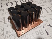
However there is no free lunch, and the Mosfet eats up about 4.2V (the Mosfet’s Vgs) in payment for doing it’s job. This is why you see a regulated rail voltage presented to the drains of the*Vfets of 19.8V (or so). An important part of the rail regulators is C1 (220uF), there to delay the arrival of this 19.8V to give the bias regulator time to ramp up. More about this here;
Power-up and power-down sequencing.
Back to depletion mode devices - The Vfets are normally on, right? We need to apply a bias voltage to control them. If the bias voltage isn’t there controlling current flow when the rail regulators power up, the Vfets will conduct an excessive amount of current and the 40-year old, completely irreplaceable smoke made from vintage Japanese un-obtainium, ground unicorn horn and pixie dust will escape. A sad result which will also smell bad.
So we must have the bias regulator working before the rail voltage is turned on.
How did Nelson do it? A simple application of the time constant to charge 2 differently sized capacitors in the regulator circuits. The regulator with the smaller capacitor will turn on before the one with the larger cap. These caps in the race are C3 (47uF) on the bias reg and C1 (220uF) on the output regulator. It’s a 4.7-to-1 ratio and C3 will be charged about 4.7 times sooner.
The TL431 are shunt regulators, so they do not conduct current until the voltage rises to the regulation value, and then they conduct so as to hold that value.
So what about power down? The rail voltage needs to be turned off before the bias voltage. (the opposite of power-up) BUT, the big cap/small cap ratio will NOT work in our favor when shutting down. It would work exactly how you’d expect, where the small cap will discharge before the big one.
So what? The VFETs will drain the supply quickly enough, but when the supply voltage drops down quickly we may find the Gate to Source voltage (Vgs) of the Mosfet at a high enough voltage to stress the transistor into failure. It's not that likely, but everyone knows that Pass wears both a belt and suspenders to hold up his pants, and this is reflected in his design.
The fix is a simple 2-cent diode. On power down, D1 will be a very attractive and very low-resistance discharge path for C1, discharging it rapidly and turning Q7 (and Q13) off, and therefore the rail voltage to the Vfets. Because there is no special path for C3 in the bias regulator to discharge, it will operate for a longer time, which is perfectly ok.
The stuff in the middle.
Ok, so far everything has been explained except for the wiggles in the center of the schematic near T16 and T17. Remember how the bias voltage regulator is set by the divider made from R11 and P1? This is a DC value but we also need to let the AC have it’s say in the circuit, as the AC is our music.
🙂 The Front-End output signal was all big and powerful the last time we left it at T18. Now this signal needs to get to the Gates of the Vfets to move our speakers, and that signal (even though it’s AC) can get pretty darn big. Big enough that it’s voltage could effect the current flowing through the regulator set resistors. The network of C5, C6 and R21 through R24 prevent the music signal from having much influence on the bias regulators. Stable bias makes for happy Vfets, so this is a good thing.
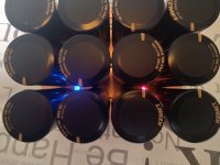
What’s left… Um… R25 R26 (221ohm) are gatestoppers for the Vfet, R33 (22.1K) adjusts the brightness of the LED (which must be blue, this is a Pass amp, after all…) and R32 (0.1ohm) gives a place to measure the output stage current. (Bias)
Global feedback is applied from the output stage from the Vfets to the Jfets through R3 (2.21K), and then R4 (332ohm) to ground.
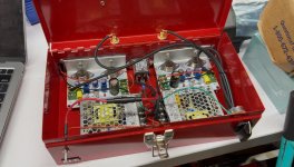
Cool! That's the basic overview of how it works. Let's build!!
😀 😀 😀
.


 So thank you all the people who helped me and especially Joe Berry who gave me the Keystone of this amp, the current generator so particular that guarantee a thermal stability
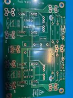
 A special thanks to gionag, my friend Rabbi Michele, who is the first to have made this amp and who made this great layout