Can someone tell me what the output impedance is on the RCA audio output?
I might also mod this thing. What are the latest recommended mods?
I might also mod this thing. What are the latest recommended mods?
I've received the oscillators I'm going to try swapping in today. I build a small board with a regulator to try on out on a Sony player I have and everything worked so I'm looking foreword to doing this to my oppo 95.
I've looked through the pages and pictures and found many people have done this mod, but I can't seem to find out what components are removed in order to make this mod work with a simple stand alone 3.3 volt regulator and clock. Can someone please guide me? I believe one of the first posts shows to remove a few components on the main board, but I can't seem to find out what to remove for the DAC clock. Also, why are these components removed?
What you saw in the beginning of this thread it refer to the main processor clock. This is another story...
The (stereo) DAC clock mod it was not treated very well here I suppose... So, I think to renew the subject here and now.
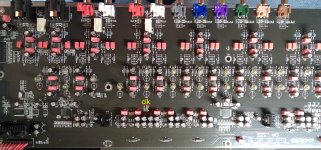
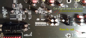
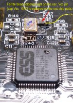
You see in the picture of the analogue board hereby, the placement of the original 54Mhz oscillator, which is common for both DACs. On the C100 near to the oscillator chip one can found the 3,3v line for oscillator power. This power it can be used to power the new oscillator. If one may use a dedicated regulator for the new clock, then a higher voltage power line should be used (regulated to 3,3v). The raw 9v rail is indicated on picture hereby.
I will suggest to not remove the original oscillator, but cut only the traces, and remove the indicated resistors. In case of malfunction, then the original approach it could be easy reestablish (reversing operations). The original oscillator may be let it work for the multi-channel DAC, or it can be dismissed if only the stereo DAC is used... Also the same clock mod it can be applied to the multi-channel DAC if need it (a second dedicated oscillator should be used).
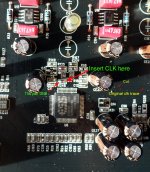
To isolate the stereo DAC clock inserting point, one should cut first the original clock trace (see picture). Then remove the resistors R248, R135 (marked x on picture). Insert the clock as shown on pictures. Coaxial cable should be used if the oscillator is placed somehow far from inserting point.
For best result, I will also suggest to solder the new oscillator directly on GND and F-out pads (to the former R248 pads), then connect the oscillator to power (eventually own regulator) by a thin (as short as possible) wire, and/or using the available power points indicated. The new oscillator chip it can be soldered in a vertical position in such case. An 0,1µ SMD cap should be soldered directly between Vcc and GND pads of the new oscillator chip. Special care should be taken while soldering operations, as the pads on board are fragile and it can be disclosed very easy. It is important to keep these pads in place, as it are very handy for the mod procedure.
Please ask if something still be unclear.
Attachments
Last edited:
Can someone tell me what the output impedance is on the RCA audio output?
I might also mod this thing. What are the latest recommended mods?
The impedance on the RCA outputs, it should be found it in original manual or datasheet of the device.
Referering to the above clock mod, if both DACs may be need it, it is up to you to experiment with dedicated oscillators for each DAC, or only one (same clock signal distributed through coaxes). If own oscillator for each DAC, some synchro issues may occur. I have not experimented myself in this direction, as I was never interested into the multi-channel stage...
Referering to the above clock mod, if both DACs may be need it, it is up to you to experiment with dedicated oscillators for each DAC, or only one (same clock signal distributed through coaxes). If own oscillator for each DAC, some synchro issues may occur. I have not experimented myself in this direction, as I was never interested into the multi-channel stage...
Thank you so much for the information. Really a huge help for installing the new clock for the DAC. With your information and pictures, I was able to complete some on my modifications today. It's certainly a step in the right direction, but it's still pretty sharp/bright sounding. This may just be something I, or someone else, will have to live with. I still have to install a new main clock, but I did install a 100 mhz saw oscillator. I swapped out a few resistors and threw in a burson v5 discrete opamp as well.
Are they any other suggestions on modifications or changes to the I/v and output stage to get a warmer sound?
Attachments
Well, I may say that changing/improving the clock signal for DAC is only a step into a enough complex process of improvements, in the trial of getting out the most of the device.
Only the DAC clock it will not bring a very dramatic improvement for resulting sound, but it will contribute to that overall improvement. If the rest of the improvements are already done, then changing the original 54Mhz clock with a 100Mhz it will bring indeed a very noticeable result.
If you appreciate the sound as sharp/bright, then it could be some not just right setup somewhere... A too brighter sound it may mean some oscillations or harmonics are present somehow into the system.
A higher clock frequency should increase the fine details in the resulting audio signal. The post DAC analogue processing it have also a crucial role for the final audio signal quality.
As I said/suggested in my previous post, if one only use the oscillator as it is, powering it from the existing power system, then the best result it could be to solder the new oscillator chip right on the available pads on PCB, without any board in between. Placing the oscillator right over the DAC chip (your approach), without any shielding/grounding in between, it may not be the very right solution... Oscillators at such high frequency have to be installed very carefully to avoid degrading the clock signal. Also the power for the oscillator it have a crucial impact over the clock signal quality. Much precautions have to be taken to avoid clock signal propagating into the power system.
As a general advise, I will recommend first a carefully analyse of the eventual modification, then choosing a final best solution as possible.
First, about the new oscillator, I will suggest you to mount it as described previously, right on the pads of the former R248 in a vertical position. Thant perforated PCB you have used to support the oscillator over the DAC chip is far from the right device in this approach, and it may worse more than improve something. Also the tantal cap for oscillator decoupling it may not be the right component in this case. Better to find a small SMD ceramic cap to solder it right on the oscillator pads.
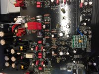
I found a picture of my old mod in this area, to illustrate my suggested approach. I have used there some very short solid wires to adapt the new oscillator footprint to the pads on the PCB. One can solder the oscillator chip in a vertical position directly to the pads on board. It will result a very solid "construction" which is much better than using a such perforated small board... A very thin and flexible wire (to not mechanically stress the oscillator chip soldered on the board pads) it will then connect the Vcc of the oscillator to the power point. A ferrite bead in between it will minimise a lot the residual frequencies to propagate into the power system. A decoupling SMD 0,1µ cap it is also recommended right on the connection point of the Vcc wire to the 3,3v trace. Such precaution and filtering are a must when handling with oscillators at these high frequencies...
Doing the clock mod in this way, one can then appreciate as finished, focusing further to the another areas of the system for improvements...
Only the DAC clock it will not bring a very dramatic improvement for resulting sound, but it will contribute to that overall improvement. If the rest of the improvements are already done, then changing the original 54Mhz clock with a 100Mhz it will bring indeed a very noticeable result.
If you appreciate the sound as sharp/bright, then it could be some not just right setup somewhere... A too brighter sound it may mean some oscillations or harmonics are present somehow into the system.
A higher clock frequency should increase the fine details in the resulting audio signal. The post DAC analogue processing it have also a crucial role for the final audio signal quality.
As I said/suggested in my previous post, if one only use the oscillator as it is, powering it from the existing power system, then the best result it could be to solder the new oscillator chip right on the available pads on PCB, without any board in between. Placing the oscillator right over the DAC chip (your approach), without any shielding/grounding in between, it may not be the very right solution... Oscillators at such high frequency have to be installed very carefully to avoid degrading the clock signal. Also the power for the oscillator it have a crucial impact over the clock signal quality. Much precautions have to be taken to avoid clock signal propagating into the power system.
As a general advise, I will recommend first a carefully analyse of the eventual modification, then choosing a final best solution as possible.
First, about the new oscillator, I will suggest you to mount it as described previously, right on the pads of the former R248 in a vertical position. Thant perforated PCB you have used to support the oscillator over the DAC chip is far from the right device in this approach, and it may worse more than improve something. Also the tantal cap for oscillator decoupling it may not be the right component in this case. Better to find a small SMD ceramic cap to solder it right on the oscillator pads.
I found a picture of my old mod in this area, to illustrate my suggested approach. I have used there some very short solid wires to adapt the new oscillator footprint to the pads on the PCB. One can solder the oscillator chip in a vertical position directly to the pads on board. It will result a very solid "construction" which is much better than using a such perforated small board... A very thin and flexible wire (to not mechanically stress the oscillator chip soldered on the board pads) it will then connect the Vcc of the oscillator to the power point. A ferrite bead in between it will minimise a lot the residual frequencies to propagate into the power system. A decoupling SMD 0,1µ cap it is also recommended right on the connection point of the Vcc wire to the 3,3v trace. Such precaution and filtering are a must when handling with oscillators at these high frequencies...
Doing the clock mod in this way, one can then appreciate as finished, focusing further to the another areas of the system for improvements...
Attachments
Last edited:
Wow. Those are some serious skills. I has super happy just to mount the clock to that board. I think we're on different levels. I'll try the decoupling cap on the clock. As far as the ferrite bead: I've seen you recommend at least a 1k in the past. I don't think I could manage a smd type though. What could I use instead?
As far as the sound: I made the resistor, capacitor and opamp change at the same time and found it to change the signature to more of what I am looking for (less bright). It's not far off now, but I still think doing something to the I/v stage would be benificial to achieve a little more body to he sound. I saw somewhere where it is completely bypassed and they circuit was changed to be have resistors to ground? Has anyone done this?
As far as the sound: I made the resistor, capacitor and opamp change at the same time and found it to change the signature to more of what I am looking for (less bright). It's not far off now, but I still think doing something to the I/v stage would be benificial to achieve a little more body to he sound. I saw somewhere where it is completely bypassed and they circuit was changed to be have resistors to ground? Has anyone done this?
You can try to get the skils too... You may remove a similar crystal from a old defect board, and exercise on it to solder a ferrite bad to a pad of it, to solder that oscillator on pads on a board, or handle with SMD components, and so on. Then you can apply the learned skils to this Oppo player improvement...
You will only need a low power (15w or lower, best temperature controlled) quite fine soldering iron, as learning to solder fast on such small devices, to not get it unnecessary heated... Well, one may need some good eyes, or some magnifier glasses for such operations...
Unfortunately it is not any alternative to that SMD type ferrite bad, if you will go this way to solder it directly to the oscillator. Any other (bigger) component it can mechanically stress the pads on that oscillator, or its body... If the components are placed on a PCB, then one can more easy experiment with différent dimensions components...
The impedance on the RCA outputs, it should be found it in original manual or datasheet of the device.
Doesn't say
Google say...
From Oppo Digital infos/specifications (105D):
• Output impedance 7.1 board L/R front channels 100Ω
• Output impedance dedicated stereo board L/R channels 100Ω
• Output impedance 7.1 board all channels except L/R front 200Ω
• Recommended amplifier input impedance is 47KΩ (Industry standard)
• Peak output level: 2.1 Vrms (RCA / Phono)
• Signal-to-Noise Ratio: >130dB (A-weighted, auto-mute), >115dB (A-weighted, no auto-mute)
• Dynamic Range: >110dBV
• Channel Separation: >110dB
It may be similar for previous models too, as the output approach it was not changed too much over time (except AC coupled outputs for newer models)...
Last edited:
Has anyone tried replacing the ess sabre 32 9018 chips with the 9028 Pro chips for the stereo and/or surround sound chip? If so, how would one rate the differences or improvement in sound?
What is the level of difficulty of replacing the 9018 with the 9028 and what tools were used to achieve replacement of the chip
The ess 9028 pro is pin and voltage compatible with the 9018.
What is the level of difficulty of replacing the 9018 with the 9028 and what tools were used to achieve replacement of the chip
The ess 9028 pro is pin and voltage compatible with the 9018.
Very subjective ... it will depend on other factors like the rest of the system.
If it's excellent, you might notice some improvement, but if not, it will be a job with no immediate results.
why the question ? the pins and the voltage also match with EssSabrePro 9038, I think.
This chip has the Sonica Dac by Oppo and I can attest that it is a very analog and detailed sound. I think that with this chip the critics to the "cold and hard" sound of the bits are finished.ery subjective ... it will depend on other factors like the rest of the system.
If it's excellent, you might notice some improvement, but if not, it will be a job with no immediate results.
why the question ? the pins and the voltage also match with EssSabrePro 9038, I think.
This chip has the Sonica Dac by Oppo and I can attest that it is a very analog and detailed sound. I think that with this chip the critics to the "cold and hard" sound of the bits are finished.
Archimago's Musings: MEASUREMENTS: Oppo Sonica DAC (ESS Sabre ES9038Pro based device)
If it's excellent, you might notice some improvement, but if not, it will be a job with no immediate results.
why the question ? the pins and the voltage also match with EssSabrePro 9038, I think.
This chip has the Sonica Dac by Oppo and I can attest that it is a very analog and detailed sound. I think that with this chip the critics to the "cold and hard" sound of the bits are finished.ery subjective ... it will depend on other factors like the rest of the system.
If it's excellent, you might notice some improvement, but if not, it will be a job with no immediate results.
why the question ? the pins and the voltage also match with EssSabrePro 9038, I think.
This chip has the Sonica Dac by Oppo and I can attest that it is a very analog and detailed sound. I think that with this chip the critics to the "cold and hard" sound of the bits are finished.
Archimago's Musings: MEASUREMENTS: Oppo Sonica DAC (ESS Sabre ES9038Pro based device)
Can someone tell me what the output impedance is on the RCA audio output?
I might also mod this thing. What are the latest recommended mods?
75 ohms is the spec output impedance. The OPPO may not be 75 ohms however.
You can certainly put a new master clock and rebuild the output stage, but the jitter will never be as low as a good reclocker like the Synchro-Mesh. I modded transports and DAC for 10 years so I know what is possible.
Now, it just does not make sense to mod in order to reduce jitter on the S/PDIF output of a transport. Just buy a good reclocker. The impedance match will be better and the jitter will be lower.
If you are on a budget, get an IFI SPDIF iPurifier for $149 USD or if you want 20ps of jitter, get the Empirical Audio Synchro-Mesh reclocker for $599:
How much jitter from a typical Transport?
And don't stop there. You will need a good S/PDIF cable with the new reclocker to maintain that low jitter. A homemade Belden 1694A cable will cut it. See how much this adds to jitter:
Can S/PDIF cable jitter be measured?
Steve N.
Empirical Audio
Pardon me if you were asking about the analog outputs. I just assumed digital, because impedance is critical there.
Steve N.
Steve N.
The ess sabre 9028 pro is advertised by ess as a drop-in replacement pin compatible with the sabre 9018.
The sabre 9038 pro is not. It carries an additional 5v input, so you could not directly perform a drop in replacement like you could when going from 9018 to 9028. I read elsewhere that the 9028 is sonically an improvement, but it does not carry a night and day difference between the two.
The sabre 9038 pro is not. It carries an additional 5v input, so you could not directly perform a drop in replacement like you could when going from 9018 to 9028. I read elsewhere that the 9028 is sonically an improvement, but it does not carry a night and day difference between the two.
What are the thoughts of putting the oscilator clocks on their own power supply, replace the 25/27 mhz crystal with a low-jitter clock crystals of the same speed, replace the 54MHz cyrstal with a 100 MHz now jitter crystal, and supply each of them their own voltage regulator of the likes of tent labs, amb, or burson. These could all be fed off of a single independent 10-12v output power supply. Surely this should improve the sound and picture.
Thoughts anyone?
Thoughts anyone?
What are the thoughts of putting the oscilator clocks on their own power supply, replace the 25/27 mhz crystal with a low-jitter clock crystals of the same speed, replace the 54MHz cyrstal with a 100 MHz now jitter crystal, and supply each of them their own voltage regulator of the likes of tent labs, amb, or burson. These could all be fed off of a single independent 10-12v output power supply. Surely this should improve the sound and picture.
Thoughts anyone?
This would improve things, however the LPS would have to be fast reacting, like Sbooster supplies. You will need good power decoupling at the crystal and buffers.
The Jitter will still be in the 100's of psec, but if you want to improve the analog outs, this is the way to do that.
Stay with the 54MHz frequency, just put a better one in there.
Steve N.
Thanks Steve N.
While we are on the subject of linear power supplies, what are the thoughts to improve things further on the dac by placing the two ess 9018 chips on their own power supply, independent from the rest of the unit? Would shunt or serial voltage regulators be in order here?
I sure wish oppo had done this. I would have paid a bit more for the unit since these improvements would bring out the very best that oppo has to offer.
Thanks Steve N.
While we are on the subject of linear power supplies, what are the thoughts to improve things further on the dac by placing the two ess 9018 chips on their own power supply, independent from the rest of the unit? Would shunt or serial voltage regulators be in order here?
I sure wish oppo had done this. I would have paid a bit more for the unit since these improvements would bring out the very best that oppo has to offer.
It's always a good idea to not share power in the DAC. I have 22 separate regulators in my DAC for instance, all based on Hynes technology. Every major chip has its own regulator, and the DAC has 2.
I was not able to get fast-reacting pass regulators off the shelf, so I designed them. They run pretty hot. You may have to use shunt to get the speed you need.
Decoupling is at least as important, maybe more. These chips need 50-100uFd low ESR electrolytic caps, good film caps of .1uFd and even smaller caps really close to the power pins. Ceramics too, but they don't help much. I like the Lelon and some Panasonic caps for the electrolytics. Forget Tantalums.
Steve N.
Empirical Audio
- Home
- Source & Line
- Digital Source
- Upgrading & modding new Oppos, BDP-93 & BDP-95