lol you are right, i was doing the (I^2 * R) with Volts, my dear God...
Yeah, I know it is hot 🙂 let's see what happens.
Yeah, I know it is hot 🙂 let's see what happens.
I hope you have sensitive speakers. The 4 Ohm power output at reasonable THD will not be very high.🙂
This is the chart we want to see. 🙂
Increase output and see how it will look. 3rd harmonics increase faster, so at some point, you'll see 3rd more than 2nd.
Increase output and see how it will look. 3rd harmonics increase faster, so at some point, you'll see 3rd more than 2nd.
No worries, Ben. I consider this to be a start of the journey. I want to build also the SIT pp and the Goldmund Nemesis. And I would also like to try after that a tube amp, I had never had a tube amp.
My "good" speakers are really non sensitive, since they are Magnepans. I have a few others and some of them are really sensitive, so I will try variations... In general I don't listen very loud and mainly "light" music, like vocals etc, no symphonic and no rock. All play on turtable, a Clearaudio Master Reference.
The amps I will build, all are going to compete against my Symphonic Line RG7 to see how this goes.
It's great. Looks like it is more powerful than FW SIT-1. How much is the bias current?
http://www.firstwatt.com/pdf/prod_sit1_man.pdf
http://www.firstwatt.com/pdf/prod_sit1_man.pdf
yeah, yeah, I know 🙁 . I found a Hammond one that could be used but different characteristics
195T5 - Hammond Mfg.
I ll put on sim to see how it goes
195T5 - Hammond Mfg.
I ll put on sim to see how it goes
I got them and they measures good. Measurement is on my 50+ watt thread.
Get them from DigiKey, if you're in US. Shipping is only $8.
Get them from DigiKey, if you're in US. Shipping is only $8.
No I live in Greece but I can get them from Germany, shipping 15 euros.
Today, Liquid cooler arrived, it is a huge devil...
Today, Liquid cooler arrived, it is a huge devil...
Hi plasnu,
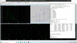
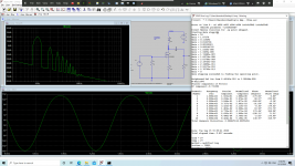
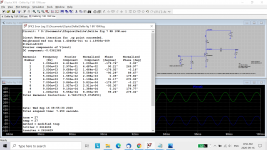
A. 1Vp input, 3.79W, 1.66% THD.
B, Pushed to the limit, 2.2 Vp input, 24W, 6,29% THD
Here are the screenshots...
I am repeating myself but I want your experiments to be safe.
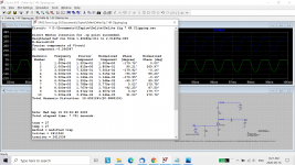
Your "B" operating point is outside of the Safe Operating Area of the device. Most builders do not push devices even close to the boundaries of Safe Operating Areas. Destruction of the device is highly likely. 270W is also a lot of heat to dissipate.
Looking at the output voltage plot, the sine wave is noticeably asymmetric. It is clipping.
I didn't check how much is the max dissipation of this particular device, but even 50% of it is high side as Ben said. Liquid cooling will make it possible? I don't know...
It's a 300W device at 25 C case temperature.
SOA charts on page 5, Figs. 15 and 16:
https://ixapps.ixys.com/DataSheet/DS100177B(IXTA-TP-TH6N50D2).pdf
SOA charts on page 5, Figs. 15 and 16:
https://ixapps.ixys.com/DataSheet/DS100177B(IXTA-TP-TH6N50D2).pdf
Ok did more homework, in the end I will learn about amplifiers.
It seems that there is always a DC negative offset, low in low input and increases as power increases. It seems also that is proportional to DC offset presenting in error log. No matter the input level, it is always there but it is 1/10th
The signal seems not to be clipping per se, although I understand that this is definitely a distortion.
I did more homework and decided to learn about the sweet spot and Vdd, Id and Vgs curves (actually to remember back from University, 20 years ago), so redesigned the circuit so that I am on the very good hotspot despite the low wattage. It proves that we have the same issue.
I then found out about bypass capacitors and also a capacitor in series with the signal in input. The in series capacitor with the signal gets things a lot better, although I did not know where exactly to put the bypass capacitor...
Maybe i will read about bypass capacitors and learn that too.
Maybe also a CS could help.
Any comments welcome.
BTW I run freq response and seems amazing to me...
Relooking the graph it doesn't seem to be a DC offset, since in t=0 V=0. So, I don't know what it is, it seems to be relieved with input capacitor..
3rd look again... reading more i am getting suspicious it leaves class A, around 4 watts anyway...
3rd look again... reading more i am getting suspicious it leaves class A, around 4 watts anyway...
Last edited:
You are correct. The output voltage waveform was not clipping but showing the effects of high distortion as you said.
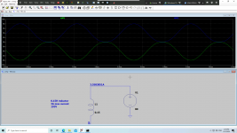
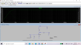
Out of curiosity, I did a LTspice simulation of the Fig. 7 circuit with choke load in place of light bulbs with both 8R and 4R speaker and I did not get any errors in the run.
I ran it at 35V and 1R source resistor which resulted in 1.5A currrent. Results were about 10W at 4.5% THD for 8R and about 5W at 4.5% THD at 4R.
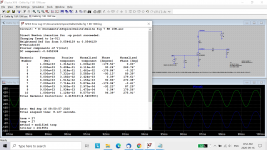
The apparent DC offset at the output must be due to something in the output coupling capacitor model. I also displayed the output voltage before and after the coupling capacitor.
Edit:
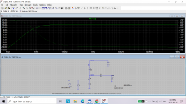
After thinking about it, the apparent offset is probably due to the V=0 axis located at the Vaverage location. The distorted sine waveform is no longer symmetrical so the horizontal axis is shifted.
I did another run showing clipping.
Out of curiosity, I did a LTspice simulation of the Fig. 7 circuit with choke load in place of light bulbs with both 8R and 4R speaker and I did not get any errors in the run.
I ran it at 35V and 1R source resistor which resulted in 1.5A currrent. Results were about 10W at 4.5% THD for 8R and about 5W at 4.5% THD at 4R.
The apparent DC offset at the output must be due to something in the output coupling capacitor model. I also displayed the output voltage before and after the coupling capacitor.
Edit:
After thinking about it, the apparent offset is probably due to the V=0 axis located at the Vaverage location. The distorted sine waveform is no longer symmetrical so the horizontal axis is shifted.
I did another run showing clipping.
Attachments
Last edited:
Clipping run attached.
Regarding leaving Class A, single ended amplifiers do not leave Class A the way push-pull amplifiers do. Overdriven single ended amplifiers can only clip.
Regarding leaving Class A, single ended amplifiers do not leave Class A the way push-pull amplifiers do. Overdriven single ended amplifiers can only clip.
Attachments
Last edited:
The apparent DC offset at the output must be due to something in the output coupling capacitor model. I also displayed the output voltage before and after the coupling capacitor.
Edit:
After thinking about it, the apparent offset is probably due to the V=0 axis located at the Vaverage location. The distorted sine waveform is no longer symmetrical so the horizontal axis is shifted.
I did another run showing clipping.
I am not sure what you mean. The apparent offset is the one we are talking about right? You mean there is no issue?
Anyway, I will run with 0.5Ohm and whatever happens. I seem to be able to deliver 15W.
Current then goes to 2.8A on coil. Maybe i will install a 3A fuse just in case.
Another question. I run the model with 50mH and 0.5Ohm internal coil and it seems OK. That means that maybe we can get other coil than 193V with lower induction?
The "apparent offset" that I referred to was the difference in +V and -V of the output voltage sine wave. I called it "apparent offset" because I think it is not due to a negative DC voltage offsetting the AC, but I believe it is due to the sine curve being affected by distortion so that it is no longer symmetric about the V=0 axis, causing the V=0 axis to shift upwards. Of course that is just my theory. I am not an electrical engineer, just an amateur diyer so I may be wrong.
Regardless of what Iq you run, you need to consider the power dissipation of the mosfet, as I mentioned many times previously.
The inductance of the load choke affects low frequency response. I did a simulation with 0.15H and 1R and another with 0.050H and 0.50R:
Regardless of what Iq you run, you need to consider the power dissipation of the mosfet, as I mentioned many times previously.
The inductance of the load choke affects low frequency response. I did a simulation with 0.15H and 1R and another with 0.050H and 0.50R:
Attachments
- Home
- Amplifiers
- Pass Labs
- Inductor Loaded De-Lite