janneman said:
With a short, the total Vin comes across the CCS. That *might* be a problem, but I can't see anything otherwise. Was it overvoltage?
Jan Didden
The problem was, that the CCS wasn't that stable, it drew more current when pulled to zero and the higher voltage drop added up to overheat the pass device.
With a cascoded pass transistor (as we have here) and R5 replaced by a FET CCS it is rocksteady.
I quickly abandoned more tests and burning more transistors, though 😉
Rüdiger
Onvinyl said:Jan, did you, or anyone else, check the step response of the reg? This can be quite disillusionary, as even a seemingly stable reg might show bad ringing or even burst out in oscillations then.
Rüdiger
No I didn't, and the reason is this. The Zout was pretty flat across frequency, as measured across the output. That indicates that the limiting factor is the layout, not the circuit. If the Zout starts low at lf, then starts to rise after a few kHz, that indicates you are really measuring the circuit, and then it can be interesting to look at the step response. I can do that when there is a new layout.
Anyways, when looking at the step response, one should limit the step rise time (or Fc) to audio frequencies. It is easy to upset any regulator (and any amp) with 1uS risetime square waves, but that doesn't tell you diddely for audio work.
Jan Didden
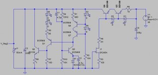
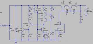
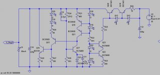
I created 3 LTSpice Model of the regulator with variations on the current source biasing D1 / D3. I did not have a model for LM334 and used a JFET that is pin-compatible, so one can actually use either. Maybe there are differences in performance to LM334, maybe not. First with a simple CCS:
Attachments
C3 and C1, etc. are starting to use sensible values.
One of the Zeners is upside down.
That last one will light up the street.
One of the Zeners is upside down.
That last one will light up the street.
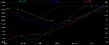
Here is the relative PSRR of the three circuits above: The series CCS is set to 100 mA, load current is 50 mA, Vin is 36V , with 1V AC, Vout is 30V. The results are interesting. Better results can be obtained with different transistors for Q5 instead (subject to quality of models):
Attachments
reduce the CCS current from 50mA to 30mA. and change the first BD to bc560c. Does that improve anything? would a 2n39xx have sufficient current capacity here?
How about changing some of the bc5x6b to bc5x0c
How about changing some of the bc5x6b to bc5x0c
Quickly: The setup is for a load current of 50 mA, and I chose the raw current through the current source as 100mA or twice the load current. I do not have models for the BC550/560 yet - I only installed LTSpice a few days ago and am still toying with it. However, I played with other resistors including some japanese models (2SC2240, 2SA970, and some others) at various positions but I only got moderate improvements if any, I will try the BC550/560 as a next step though.
The only position that made a substantial difference is Q5. I tried a BC327-40 and got extended bandwidth, probably from lower Cob ? (BC550/560 should have similar results) Then I tried a 2N4403, this lowered the PSRR by another 10-15 dB. Since Q5 has not too much voltage across it you can get away with using TO92 packages with currents of at least 150 mA.
Values of -160dB are somewhat suspicious, but then I saw Glen's grahs and they go down even further.
One of the Zeners is upside down.
You are right, I will correct this. If you see other bobos let me know. Surprisingly I tested one setup with a 12V ideal voltage source and got identical results.
Edit: I quickly turned the Zeners around but for some reason it does not change anything
 - either the program corrected this "somehow" or there is another fault ? But the 12V voltage source that I tried in place of the Zener did not change the curves either.
MRupp said:The next version has a cascoded CCS, this works both with the JFET and the LM334 (see datasheet).
Martin,
I would keep the two current sources for biasing apart. You don't want any ripple in the series CCS to end up in the shunt part.
A simple change that may improve regulation is to run R10 not to ground, but into the top of the zener. That way, you further stabilize zener (ref) voltage against Vout variations. R10 would then be smaller (would be anyway) but you could also replace R10 with a ccs. The FET type would be OK, I just had some LM334's laying around, that's why I used that one.
As far as the sims, they are OK to compare things, but don't get to excited with absolute numbers. For one thing, it doesn't take into account the layout and a lot of other real-world issues, for another, you don't really know how realistic the models are.
I think it is time to fix the circuit and move on to the pcb.
Jan Didden
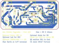
A different pcb layout approach to the current design, but illustrates the earthing focus on the O/P terminal - it does include some of the "J.D" upgrades, but not the last "rail-to zener" resistor that is currently under discussion.
Jan,
This resistor from the o/p rail to the top of the zener/Q3 emitter ....
If I follow your last post correctly, we can lift the gnd connection of the R10 (or R20 in the 2nd diagram) and attach this to the top of the zener, or even better, convert it to a BF246+R CS? This then is connected directly across the Q3 be junctions?
Martin,
On the first diagram, the Q2 emitter resistor is set as 1R0 but on the next 2, is a 10R - a misprint? (ie 0.1R)?
Attachments
Martin, I would keep the two current sources for biasing apart. You don't want any ripple in the series CCS to end up in the shunt part.
I fundamentally agree, but this just looked too good - I may pursue this topology a little further outside this project. Btw., it is just combining the LED strings of both CCS. The second CCS is actually relying on the fact that the first CCS isolates it / and the whole regulator part from the rails. I also tried a CCS to bias the second string of LEDs but this brought no improvement whatsoever.
I think it is time to fix the circuit and move on to the pcb.
So the question goes back to the whole team, what's next?
jameshillj said:A different pcb layout approach to the current design, but illustrates the earthing focus on the O/P terminal - it does include some of the "J.D" upgrades, but not the last "rail-to zener" resistor that is currently under discussion.
Jan,
This resistor from the o/p rail to the top of the zener/Q3 emitter ....
If I follow your last post correctly, we can lift the gnd connection of the R10 (or R20 in the 2nd diagram) and attach this to the top of the zener, or even better, convert it to a BF246+R CS? This then is connected directly across the Q3 be junctions?
Martin,
On the first diagram, the Q2 emitter resistor is set as 1R0 but on the next 2, is a 10R - a misprint? (ie 0.1R)?
Sorry, my mistake: I meant R2, 10k, that biases the D2/D4 string for the shunt cascode. This bias current now goes to gnd. My proposal is to 'use' it to stabilize the Vref by returning it to the top of the ref zener. Next step would be to replace this R with a ccs.
Jan Didden
Martin, On the first diagram, the Q2 emitter resistor is set as 1R0 but on the next 2, is a 10R - a misprint? (ie 0.1R)?
Fundamentally yes: The Q2 emitter resistor value can be varied. For BJTs 1-2 Ohms seems to be fine and a lower value did not show much improvement.
Since the pinout of Q2/BD139 is equivalent to that of TO220 MOSFETs, e.g. IRF610 (BCE VS GDS) I played with both. For IRF610 0.1 - 0.2 Ohms seemed about optimal (the bias resistor was then set to 400 - 800 Ohms to allow 4 Volts at 5 - 10mA). My simulations where based by having an AC current component on the load (50mA fixed, 5 mA sine current sweep).
I cannot give a fuller answer since I do not have access to my home PC (and not much time right now).
janneman said:
What do you think Glen?
You're poking in the dark unless you do a loop gain plot. The loopgain2.asc example file that comes with LTspice has a handy loop gain probe.
Cheers,
Glen
G.Kleinschmidt said:
You're poking in the dark unless you do a loop gain plot. The loopgain2.asc example file that comes with LTspice has a handy loop gain probe.
Cheers,
Glen
Err... yes. I was hoping for a well-educated guess from a well-experienced designer 😉
Jan Didden
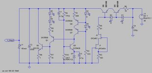
corrected version
Here is my corrected and final version, with the cascoded current source as I would implement it, but I am off course not the owner of this project. R5 is still left in to allow higher voltages than J3 can take. Do not get too hung up on the particular JFets, bjts, and resistor values, there is still some room to tweak, e.g. if a particular part cannot be obtained:
Here is my corrected and final version, with the cascoded current source as I would implement it, but I am off course not the owner of this project. R5 is still left in to allow higher voltages than J3 can take. Do not get too hung up on the particular JFets, bjts, and resistor values, there is still some room to tweak, e.g. if a particular part cannot be obtained:
Attachments
- Status
- Not open for further replies.
- Home
- Amplifiers
- Solid State
- Bipolar discrete shunt regulators