Re: corrected version
Martin,
Please put your LTSpice model up for download.
Thanks
Jim
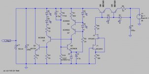
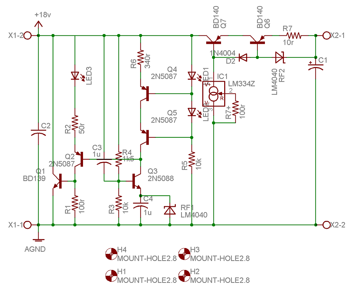
MRupp said:Here is my corrected and final version, with the cascoded current source as I would implement it, but I am off course not the owner of this project. R5 is still left in to allow higher voltages than J3 can take. Do not get too hung up on the particular JFets, bjts, and resistor values, there is still some room to tweak, e.g. if a particular part cannot be obtained:
Martin,
Please put your LTSpice model up for download.
Thanks
Jim
Please put your LTSpice model up for download.
Will do but not sure if I will have time this evening.
Only comment I have is to connect bottom of R2 to emitter Q3 instead of to ground.
Changed, and Netlist added:
Attachments
Next step would be to replace this R with a ccs.
"In my simulations" - ideal CCS at 8mA - this does not change the PSRR, and improves the output impedance very slightly, less then 1 dB. But either the models suck or I am not testing the output impedance correctly, or it really does not do much.
MRupp said:
"In my simulations" - ideal CCS at 8mA - this does not change the PSRR, and improves the output impedance very slightly, less then 1 dB. But either the models suck or I am not testing the output impedance correctly, or it really does not do much.
Martin,
It will have more impact with low Vout, like +5V reg. Then, R2 gets much lower and acts less and less as a CCS.
Can you look at that in your sim?
Jan Didden
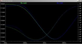
Here is the graph showing output ripple suppression, if that is the right word. I set the AC load to 50mA standing current and 5mA AC current, Vin is now 12V AC 0V DC. The curve looks strikingly similar to the first, so maybe I am not measuring the right thing ?
Attachments

Another suggestion: what would happen if we move D1/D3 current sink from ground and tied it to regulator output? We could change it to the simple one J-fet CCS, and I think the current loop would be shorter? Could we face some regulator start up problem if we do so?
MRupp said:Here is the graph showing output ripple suppression, if that is the right word. I set the AC load to 50mA standing current and 5mA AC current, Vin is now 12V AC 0V DC. The curve looks strikingly similar to the first, so maybe I am not measuring the right thing ?
Martin you mean Vin = 12V DC and 0V AC?
Jan Didden
aparatusonitus said:Another suggestion: what would happen if we move D1/D3 current sink from ground and tied it to regulator output? We could change it to the simple one J-fet CCS, and I think the current loop would be shorter? Could we face some regulator start up problem if we do so?
The current through D1/D3 contains (a lot of) ripple current. You would be injecting it into the output. I can see only disadvantages.
Jan Didden
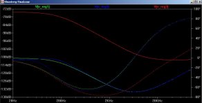
Here the last suggestion, looks much worse, curve in red.
Jan, for the first diagram (PSRR) I set Vin 12 V DC and 1 V AC, for the second diagram I added 5mA AC load current (output load I1 and 2, both already set to 50 mA DC current) and changed the Vin AC component to 0 Volts, not that it did change the curve in any way but I thought this might be a cleaner cut between the two situations. Hope this answers it ? I just wonder if there is another way to measure these values.
Martin you mean Vin = 12V DC and 0V AC?
Jan, for the first diagram (PSRR) I set Vin 12 V DC and 1 V AC, for the second diagram I added 5mA AC load current (output load I1 and 2, both already set to 50 mA DC current) and changed the Vin AC component to 0 Volts, not that it did change the curve in any way but I thought this might be a cleaner cut between the two situations. Hope this answers it ? I just wonder if there is another way to measure these values.
Attachments
sims
Would you be so kind to simulate up to MHZ range so we can see what goes there. Can we include at the input some ferrite or small inductor (100u to 1mH) to improve high frequency behaviour?
Regards,
Pred
Would you be so kind to simulate up to MHZ range so we can see what goes there. Can we include at the input some ferrite or small inductor (100u to 1mH) to improve high frequency behaviour?
Regards,
Pred
MRupp said:Here the last suggestion, looks much worse, curve in red.
Jan, for the first diagram (PSRR) I set Vin 12 V DC and 1 V AC, for the second diagram I added 5mA AC load current (output load I1 and 2, both already set to 50 mA DC current) and changed the Vin AC component to 0 Volts, not that it did change the curve in any way but I thought this might be a cleaner cut between the two situations. Hope this answers it ? I just wonder if there is another way to measure these values.
No you measure OK, but in your earlier post you said "Vin to 12V AC and 0V DC", I thought that was a typo and you confirmed that.
I guess in both cases you measure at Vout, of course.
Now, why would the curves swing up after 20kHz or so? Not a big issue, just wondering.
Jan Didden
Only saw my typo after the reply.
I am stealing my time from somewhere else and cannot do more sims right now. You have the netlist and are welcome to try yourself. The frequency limit was set to better show the differences at low frequencees, they even out in the MHz range, basically you have the upward slope into the 10s of MHz. I inserted a 1 mH / 5 Ohms inductor after the CCS and before the actual shuntreg. It does indeed improve PSRR as expected but shows a resonance peak. So yes, can be done but we need to look into damping this. Suggestions are welcome.
Would you be so kind to simulate up to MHZ range so we can see what goes there. Can we include at the input some ferrite or small inductor (100u to 1mH) to improve high frequency behaviour?
I am stealing my time from somewhere else and cannot do more sims right now. You have the netlist and are welcome to try yourself. The frequency limit was set to better show the differences at low frequencees, they even out in the MHz range, basically you have the upward slope into the 10s of MHz. I inserted a 1 mH / 5 Ohms inductor after the CCS and before the actual shuntreg. It does indeed improve PSRR as expected but shows a resonance peak. So yes, can be done but we need to look into damping this. Suggestions are welcome.
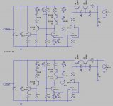
Sorry guys, took a while to get the time to work on this at all. Here is a preliminary layout, basically following what (I think) Jan suggested.
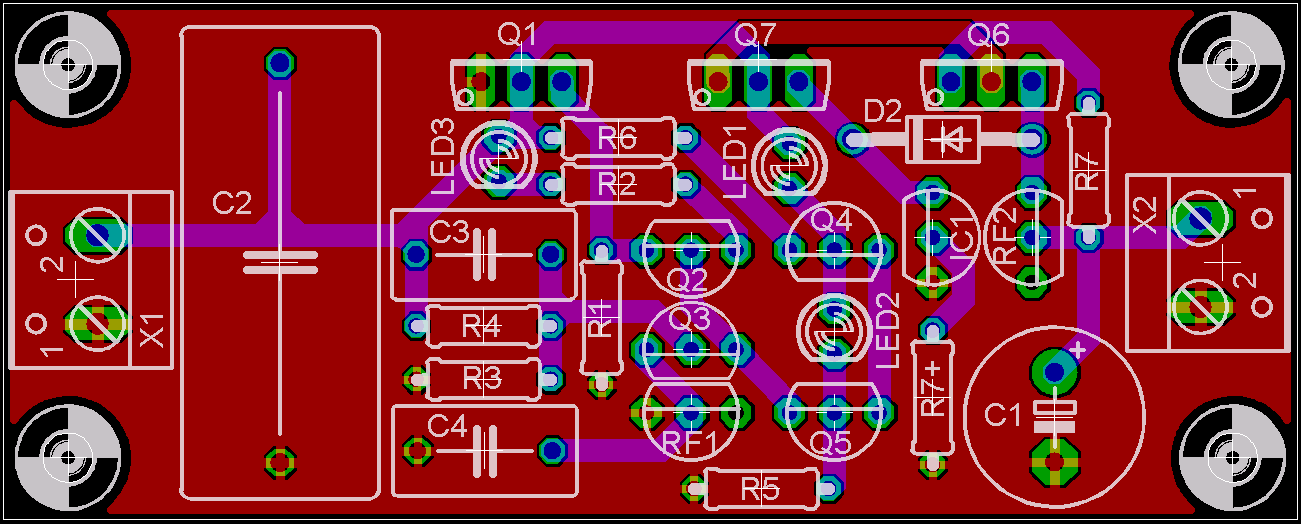
janneman: Use both layers to get short direct tracks, forget about the gnd plane, won't help anyway.
Have fun, Hannes
I agree, get rid of the ground plane.
Use a star connected ground point that coincides with the output ground.
And make sure that the output live is also a star connected point that coincides with the output live. As an example look at the route from LED1 to the output, how many other devices are sharing that trace?
The sense traces leads could be done as links and that leaves the option to take the sense leads to a very close load PCB (one stacked above the other).
- Status
- Not open for further replies.
- Home
- Amplifiers
- Solid State
- Bipolar discrete shunt regulators