Just asked for another experienced mind to join us.... hope he cares to do so 🙂
Great minds think alike (I think 🙂)
https://www.google.com/search?q=gre..._7xCoSlPZajgJgL&ved=0CEEQsAQ&biw=1680&bih=962
Great minds think alike (I think 🙂)
https://www.google.com/search?q=gre..._7xCoSlPZajgJgL&ved=0CEEQsAQ&biw=1680&bih=962
Great minds discuss ideas
Average minds discuss events
Small minds discuss people
When you surround yourself with great thinkers, you will become a great thinker! It seems to be osmose 🙂
That is why I want to follow your thoughts Frans.
Last edited:
How can I implement a CFP VAS ?
Replace Q18 by a complementary-feedback-pair. But think about it? is it needed (in this stage) to complicate things? how is it as it is how? (the last 'how' was added for symmetry, but then it complicated the sentence, you could ask yourself 'was it needed?' and 'how is it as it is how?') 🙂
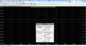

I set CM = 47pF and I get 70 degre phase margin.
But I still don't understand, why THD 20 is high. See attachment.
Just checked the schema from post #84 and it does not show this THD.
Check the bias current in your configuration (or redo your testing with #84).
Just checked the schema from post #84 and it does not show this THD.
Check the bias current in your configuration (or redo your testing with #84).
Bias current around 53mA. Please see my simulation.
Attachments
Hi bimo
Welcome a thank you for your intervention.
Unfortunately I do not have the trannies you used in my library.
Would you care to do the same sim using the stock components in my schematic (post 84)?
Bias current should be around 180mA in each output transistor.
Welcome a thank you for your intervention.
Unfortunately I do not have the trannies you used in my library.
Would you care to do the same sim using the stock components in my schematic (post 84)?
Bias current should be around 180mA in each output transistor.
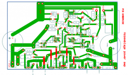
Oops 🙂 clipper message posted here http://www.diyaudio.com/forums/analogue-source/218625-paradise-builders-359.html#post4013785
Read all about it 🙂
Read all about it 🙂
Hi Ricardo,
I would recommend that you use other type of output transistors, (D44h/D45H) have very bad S.O.A (safe operation area) at 35 Volts they can only take 400mA, for example a NJL3281D can take 6A for 1 second at 35 volts and 4A at DC, almost all audio transistors from toshiba, sanken, on, fairchild or magnatec have very good S.O.A. and will be more reliably.
Other thing that I strongly recommend is the use of a small inductance (1uH) in parallel with a 4.7 resistor at the output of the amplifier, not using this inductance is a mistake that I have made myself some year ago, the capacitance from the speakers cables can make the amplifier oscillate, this oscillations are difficult to spot but the sonic degradation is very audible, I only discover that problem because when I where using one type of speaker cables the sound was very good but switching to other cables the sound become more fatiguing and veiled, adding the output inductance on that amplifier resolve the problem and the amplifier sounded much better.
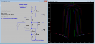
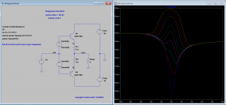
Other thing that I would like to show is this images that represent the gain of the CFP pair and the gain of an emitter follower with a 4R load at various quiescent current values, as one can see the CFP pair have an abrupt change in gain at the crossover region.
Attachments
Hi Sergio
I need some explanation to fully understand the graphs you sent me.
Can you point me some more suitable output transistors that have only three legs ?
I need some explanation to fully understand the graphs you sent me.
Can you point me some more suitable output transistors that have only three legs ?
You can try MJL3281A (NPN) MJL1302A (PNP).
the spice models can be found in Bob Cordell page:
CordellAudio.com - SPICE Models
the spice models can be found in Bob Cordell page:
CordellAudio.com - SPICE Models
As far as i understand a simple EF stage has lower gain change in the crossover region then a CFB stage.
The CFB stage has that gain change in a more narrow region though.
Sergio, in your simulation two resistors are missing that are in Ricardos amp.
I do not know if that makes any difference.
It could be beneficial to put emitter resistors to PSU in the output transistors.
The CFB stage has that gain change in a more narrow region though.
Sergio, in your simulation two resistors are missing that are in Ricardos amp.
I do not know if that makes any difference.
It could be beneficial to put emitter resistors to PSU in the output transistors.
- Home
- Amplifiers
- Solid State
- Assemblage Power Amp