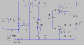
After building the Nobrainer power amp designed by Joachim Gerhard modded according to FdW ideas JG´s Nobrainer and Nobrainer Discrete - Page 33 - diyAudio I want to build a special version using a singleton input stage and double output devices so I can have more power and also verify the differences relative to the original opamp input.
Following Bigun work I asked his permission to use his input stage TGM8 - an amplifier based on Rod Elliot P3a - diyAudio
The resulting schematic sims ok but I would like to have the experts input regarding numerous doubts I have.
For reference I am posting the LTspice file as well as an initial schematic.
6 years ago I started this thread to develop a SE IPS power amp.
Now I am presenting the final evolution, the P200 model that uses Laterals on the output and a sziklai cascoded and ccs loaded on the input.
Attachments

Last edited:
I will now provide a basic explanation of the circuit to ease newcomers reading.
The input stage uses a singleton layout Q4 being the input transistor.
Q8 R23 R24(trimmer) and D1 form a biasing that enables nulling output offset.
Quoting BIGUN "Singleton does not have good temperature stability and if you want to remove the input cap like I do, then you need to d.c. bias the feedback network to allow for the Vbe drop between base-emitter of the input device. I've used a zener diode to create a negative reference voltage independent of the supply rail voltage. From this I've created a voltage divider from the zener reference to ground using a resistor and a transistor wired as a Vbe multiplier. By adjusting the Vbe multiplier I can change the d.c. bias fed into the feedback network and thereby set the d.c. offset at the amplifier output. The Vbe multiplier that is part of this biassing provides temperature compensation for the input stage."
Q13 Q15 Q16 Q17 R12 R19 R27 R30 form FdW very stiff CCS that feeds the mirror (Q1 Q3 Q9 Q10) that provides current to the Vbias circuit.
The Vbias circuit (Q14 Q5 R29 trimmer) presents my initial doubt: Do I need a third transdiode Q2 or can I leave it out ?
What should be the ideal voltage feeding the bases of the drivers Q12 Q6 ?
Do I need the base stoppers R48 R49 for the drivers ?
Collector and emitter resistors are 22 ohm to enable the drivers to work at around 30mA... Do I need to heatsink the drivers ? (I would not like to use the same heatsink for the drivers and the output transistors because this is a CFP configuration.
More questions to follow.... many more 🙂
Two Vbe drops, two diodes in bias.The Vbias circuit (Q14 Q5 R29 trimmer) presents my initial doubt: Do I need a third transdiode Q2 or can I leave it out ?
IME you are much more flexible WRT choosing driver and output quiescent currents and resistor values when using a Vbe multiplier though. Diode bias is pretty much extinct nowadays. Trim pot goes in the base-emitter leg.
Possibly. Unless you have accurate transistor models, you may not be able to assess that in simulation.Do I need the base stoppers R48 R49 for the drivers ?
Defo. Almost 35 V at 30 mA is over 1 watt, an uncooled TO-126 would run very hot like that.Collector and emitter resistors are 22 ohm to enable the drivers to work at around 30mA... Do I need to heatsink the drivers ?
I'd put them on a common heatsink along with the bias Vbe multiplier transistor, and make sure that the direct connections between the drivers and Vbe multiplier are as short as possible. (Heat conduction in metal is a lot faster than die --> case --> heatsink --> case --> die.)
D2-D5 are not going to help your linearity. I would also consider using an output inductor. RC zobel resistor could also be reduced to 4.7 ohms.
Last edited:
Member
Joined 2009
Paid Member
I agree, the diode clamp on the input is risky - the diodes will have some conduction at reasonable signal levels and add distortion. If a clipper is important to you then you should search out the 'klever klipper' by Bob Cordell.
I'd add the provision for compensation capacitors on each output CFP driver, base-emitter. You don't have to install them but you want the option.
I'd add the provision for compensation capacitors on each output CFP driver, base-emitter. You don't have to install them but you want the option.
HI
Could you share the .mod include in your schematic ?
Thanks
Hope this is it:
Attachments
Two Vbe drops, two diodes in bias.
Trim pot goes in the base-emitter leg.
Thank you for your input.... you refer to the trim pot connections if I use a Vbe multiplier, right ?
I agree, the diode clamp on the input is risky - the diodes will have some conduction at reasonable signal levels and add distortion. If a clipper is important to you then you should search out the 'klever klipper' by Bob Cordell.
I'd add the provision for compensation capacitors on each output CFP driver, base-emitter. You don't have to install them but you want the option.
You are right.... I found the diodes increase third harmonic distortion in the simulator.
I will search for Cordell's klever klipper.
I need a clipper because my initial build is quite sensitive to input bursts to the point of burning the output drivers 🙁
Here you have 1st revision including a Vbe multiplier, the compensation caps on the drivers, no clamping in the input and a revised input GND.
It sims ok but I am not really sure about the Vbias layout.... is it feasible ?
About the output coil in series with the output... what value ?
It sims ok but I am not really sure about the Vbias layout.... is it feasible ?
About the output coil in series with the output... what value ?
Attachments
Here you have 1st revision including a Vbe multiplier, the compensation caps on the drivers, no clamping in the input and a revised input GND.
It sims ok but I am not really sure about the Vbias layout.... is it feasible ?
About the output coil in series with the output... what value ?
Best to use a transistor that can be mounted on the heat sink, like a BD139, for the Vbe multiplier.
There is no need for ground-lifting, just make sure (when designing a PCB, or doing the cabling) that you have one ground point, no loops, and all circuit points that need ground are using a separate wire.
Also break ground loops at the input connector, isolate the connector from the case (mount it on a peace of Plexiglas) and connect the input ground to the star-ground-point using a 10 Ohm resistor (also check the Paradise grounding instructions/plans/guidelines).
Check D.Self's book on PSU design considerations.
Hi
why not using a diamand buffer with tour CFP ?
Why not ?
Can you post a schematic ?
Incredible.
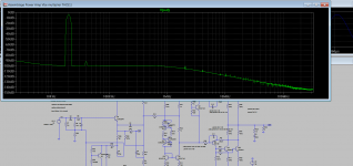
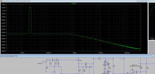
Following your instructions I got the following THD:
As far as I can see, you've got gain = 1 here (100% GNFB) - in this case this kind of level of distortion is no surprise 😉
The reason is R7 = 1 mohm (0.001 ohm). It will not work this way in real life 🙁
Cheers,
Valery
Optional driver compensation caps should go from base to collector, which makes them far more effective (Miller effect).
Use a Kaiser-Bessel window with Beta of about 20 for your FFT.
I assume the transistor types are placeholders? BC337 would be very bad in a VAS, for example (very low Early voltage) - BF470 and relatives work far better. Likewise, 2N/TIP3055 really suck in terms of beta droop.
Douglas Self has shown that a singleton input contributes copious distortion; I'm not really sure how to tackle that (you can't really give the thing a current source, can you?).
Last edited:
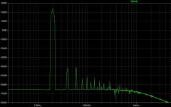
Continuing post #17, if we set R7 to 1 MEG (this is what, I assume, you meant it to be), the spectrum becomes more realistic 🙄
Ahhhh 🙂 I did not see that, but (the original value) show as 1 milli ohm 🙂 One must be aware that LTSpice is case insensitive and uses 'M' (or 'm') for Milli and 'MEG' (or 'meg') for Mega.
Last edited:
- Home
- Amplifiers
- Solid State
- Assemblage Power Amp