I did Lt Spice simulation of this amp. asc file attached.
I did not try yet to fix anything but, there is something wrong with this amp - unless my sim is not correct, please verify.
If simulated 'as is':
a) there is 15V DC offset at the output (with 20V rails)
b) lower output device idle current is 490mA, while upper one is 2.5A
So these results are consistent with Chermann's 'real world' results.
Christian - you didn't do anything wrong 🙂
I'm afraid that this amp was not well designed, or there are some mistakes in the schematic, and no one bothered to simulate it.
Perhaps this can be fixed. I suspect the biasing circuit to not to work as it's supposed to.
All models are included in the sim so it can be easily run.
With 24V rails the difference between upper/lower outputs' current is even bigger...
One obvious solution would be to replace 3 transistors responsible for Bias, and replace them with traditional Vbe multiplier with 1 transistor.
But I guess that's was the whole point of aa14 - smart biasing based on monitoring output current over emitter resistors.
Not sure why that was even needed for a class A amp...
Attachments
Last edited:

THANK you very much Minek for your work and Eric for kind words.
I have no problem that i do something wrong...but as you said...the amp is not working in the sim too.
i am actually busy with a ACA linear power supply for my friend....so i am not lazy 😉
I have no problem that i do something wrong...but as you said...the amp is not working in the sim too.
i am actually busy with a ACA linear power supply for my friend....so i am not lazy 😉
Hi
i have got 1mV DC offset if i have just T1,T3, T6, T7 +T8 is inside the PCB other Transistors are out! 🤣
I have the thinking that the automatic bias is influencing the IPS and that is not good. if i remember right in the very first time if i do not care about the heat of the transistors i see that the auto bias is working. i did a comment at the first posts.
never the less with DC offset of VOLTS at the speaker it is not nice.
hi minek
happy new year to all members...a specially to minek😉
i learn a bit LT spice..😊
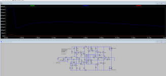
your sim shows a sinus wave but with a 15Volt DC offset !!! yes i can confirm that.
i did a simulation with input shorted and i add a 0,01R and 100mF cap at your power supply to look at some ramp up.
i played around with the ramp and voltage to look at maybe stable output (= less DC offset) but without positive result. the amp is reacting the same.
but if i short the input instead of your input generator i got 0Dc offset.
yellow is Vout
blue is base of Q11
red is base of Q12
Q11, Q12 are the sensing transistors which take the voltage from the Emitter resistors for automatic biasing. but why is the base of the positive rail so high and the negativ current or base voltage so low?
chris
happy new year to all members...a specially to minek😉
i learn a bit LT spice..😊
your sim shows a sinus wave but with a 15Volt DC offset !!! yes i can confirm that.
i did a simulation with input shorted and i add a 0,01R and 100mF cap at your power supply to look at some ramp up.
i played around with the ramp and voltage to look at maybe stable output (= less DC offset) but without positive result. the amp is reacting the same.
but if i short the input instead of your input generator i got 0Dc offset.
yellow is Vout
blue is base of Q11
red is base of Q12
Q11, Q12 are the sensing transistors which take the voltage from the Emitter resistors for automatic biasing. but why is the base of the positive rail so high and the negativ current or base voltage so low?
chris
Attachments


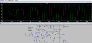
I managed to see a sinus output on this amp - sim time has been extended to 20ms, because this biasing circuit needs some time to kick in.
Once it settles, amp shows proper output.
Problems:
a) original gain of the amp (defined by R15 and R5) was too high. Increased R5 to 2k.
b) there is visible crossover distortion in the output
c) there are ugly current spikes on pretty much every transistor in this amp.
All of this is caused I think by bad biasing subsystem (Q11, Q12, Q13).
I think the best solution would be to track down which commercial amp mr. Apex used as an 'inspiration' for AA14, and look at the original.
These self-biasing circuits are usually more complex than what we see here, so perhaps Apex simplified something in it in a wrong way.
Or do what printnik did and remove this biasing subsystem completely, and replace it with traditional Vbe multiplier (which normally is not needed in A class amps). The whole (and only?) interesting thing about AA14 was the novelty biasing circuit; without it - it's totally 'normal' amp, that might not be worth building, given all these troubles so far, unless someone puts some time to sim it properly.
Attachments
Hi you, !
Thank you printnik for your suggestion. i will try this in my sim.
you did a VBE multiplier as minek proposed - that is working fin - thanks!
chris
Thank you printnik for your suggestion. i will try this in my sim.
you did a VBE multiplier as minek proposed - that is working fin - thanks!
chris
thanks minek...i will learn about LTspice...i will use the AA14 as learning an try my best.
hopefully you and printnik like to support me for that 😉
hopefully you and printnik like to support me for that 😉
Hi minek
as i can follow you you change is:
R5 from 1k to 2k and discard the D1 (iPS) completely and everything is fine,
.... except of your described artefacts of ugly current spikes
...and the crossover distortion..its visible
your file is called "correction_minek"
this spike? Ie16 (Q16)
as i can follow you you change is:
R5 from 1k to 2k and discard the D1 (iPS) completely and everything is fine,
.... except of your described artefacts of ugly current spikes
...and the crossover distortion..its visible
your file is called "correction_minek"
this spike? Ie16 (Q16)
Attachments

Last edited:
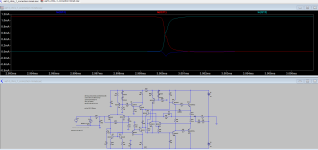
so i checked the emitter current at the bias setting transistors- Q11, Q12, Q13.
so the distortion is that ?
sorry i am a noob in LT spice and amp 😉
the pcb are ready build and why not.....but i want to have a BJT class a amplifier just for testing and listening...try the AA14...
so the distortion is that ?
sorry i am a noob in LT spice and amp 😉
the pcb are ready build and why not.....but i want to have a BJT class a amplifier just for testing and listening...try the AA14...
Attachments
Last edited:
hi
printnik VBe multiplier shows no crossover dist. after 20ms. so fine so good
mineks version with add D1 and D7 is still the same - crossover dist still visible at ramp up (20ms)..ooookay
printnik VBe multiplier shows no crossover dist. after 20ms. so fine so good
mineks version with add D1 and D7 is still the same - crossover dist still visible at ramp up (20ms)..ooookay
Hi printnik
is there a reason that you made different values for R12 (pos. rail 360R) and R14(neg. rail 82R) ??
is there a reason that you made different values for R12 (pos. rail 360R) and R14(neg. rail 82R) ??
hi
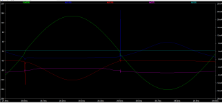
i playing around...sorry that i am not able to be better.
i check the unsymmetrical gain what printnik wrote.
at Vout you will see a peak + 14,89Vp and - 16,17Vp (R12,R14 220R) and that the negativ rail transistor behave like minek wrote. --> spikes
strange that Q9 is doing nothing and the Q7 sipkes
Attachments
Last edited:
hi again
i played With R12 and R14 . R12 360R and R14 260R is nearly the same.
gain is with minek setup 21,58dB gain.with V input 1,5V you get the maximum un-clipped output with 24V rail = 18V symmetrical.
can you confirm this printnik?
spikes are still here...no idea
i played With R12 and R14 . R12 360R and R14 260R is nearly the same.
gain is with minek setup 21,58dB gain.with V input 1,5V you get the maximum un-clipped output with 24V rail = 18V symmetrical.
can you confirm this printnik?
spikes are still here...no idea
Attachments
- Home
- Amplifiers
- Solid State
- Apex AA14 Amp Class A 24V Supply