Hi
Next Project an the way")
APEX AA14 - Class A amp...Prasi did excellent documentation. !! THX!
Gerber file : post #3
I want to try this amp but as i realized that nobody built this i want to ask in a separate Thread, because in the 100W Ultimate Fidelity Amplfier thread it is too mixed.
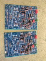
my build:
pcb in HASL standard quality - blue
because of try out some BJt transistor(BC557, KCS1845, ...etc....) and BD140...(3503/1381.....TTA...) i used pin header female - looks strange but...
As C1 i used a Nichicon Muse BP 10µF, As C4 i use a FKP2 Wima (FKP2G001001D00JSSD)
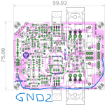
Don´t forget to wire an extra cable from GND signal input to the Power GND- its written on the top right corner on the bare PCB.
my question regarding caps.
because of avoiding some bad influence because of wrong caps - maybe too big capacitance i kindly ask:
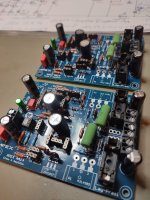
C6, C9 are nichicon UKZ 100µF/25V UKZ
C3, C7, C12, C13, are 180µF/50V 105C Panasonic EEU-FR1H181L
Q1, Q2 :For the output transistor i plan 2cs5200 and SA1943
T14/T15 Driver MJE15028G NPN, MJE15029G PNP
help and comments are welcome .
thanks
chris
8.11.2023 edit: C4, - C6,C9 andC3,C7, C12, C13 updated
10.11.2023 edit: Driver T14/T15 correction, gerber file post#3
1.2.2024: edit: Amp is working with remove of D1
remove D1
change the value of R8 from 1k5 to 2k (2k2) - lower the gain to about 21dB
use a Thiele Network at the output (0,5µH //3R3 is working - Thiele Network
Next Project an the way
APEX AA14 - Class A amp...Prasi did excellent documentation. !! THX!
Gerber file : post #3
I want to try this amp but as i realized that nobody built this i want to ask in a separate Thread, because in the 100W Ultimate Fidelity Amplfier thread it is too mixed.
my build:
pcb in HASL standard quality - blue
because of try out some BJt transistor(BC557, KCS1845, ...etc....) and BD140...(3503/1381.....TTA...) i used pin header female - looks strange but...
As C1 i used a Nichicon Muse BP 10µF, As C4 i use a FKP2 Wima (FKP2G001001D00JSSD)
Don´t forget to wire an extra cable from GND signal input to the Power GND- its written on the top right corner on the bare PCB.
my question regarding caps.
because of avoiding some bad influence because of wrong caps - maybe too big capacitance i kindly ask:
C6, C9 are nichicon UKZ 100µF/25V UKZ
C3, C7, C12, C13, are 180µF/50V 105C Panasonic EEU-FR1H181L
Q1, Q2 :For the output transistor i plan 2cs5200 and SA1943
T14/T15 Driver MJE15028G NPN, MJE15029G PNP
help and comments are welcome .
thanks
chris
8.11.2023 edit: C4, - C6,C9 andC3,C7, C12, C13 updated
10.11.2023 edit: Driver T14/T15 correction, gerber file post#3
1.2.2024: edit: Amp is working with remove of D1
remove D1
change the value of R8 from 1k5 to 2k (2k2) - lower the gain to about 21dB
use a Thiele Network at the output (0,5µH //3R3 is working - Thiele Network
Attachments
-
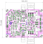 AA14 lay-r5.png71.9 KB · Views: 858
 -
aa14 r5-bot cu.pdf82.8 KB · Views: 131
-
aa14 r5-top silk.pdf64.4 KB · Views: 110
-
 AA14 sch-r5.png10.1 KB · Views: 892
 -
 Apex_AA14_amp_ClassA_1.jpeg354.2 KB · Views: 836
 -
 Apex_AA14_amp_ClassA_2.jpeg412.4 KB · Views: 445
 -
 Apex_AA14_amp_ClassA_3.jpeg483.5 KB · Views: 499
Last edited:
For T14/T15 i use the MJE15028G NPN and i did a hfe measurement. because of the peaktec DCA pro is not able to provided more then 5mA i build a test rig for measure the hfe.
the transistors get warmed up at a heated heat sink to simulate the the "real" world about 40°C.
i setup the Ic to about 90mA and then let them run 30-40seconds to heat them up completely.
then the current ´s and voltage was measured.
here is my actual list of hfe. the colors help be for better choice .
pnp in the next few days.
have fun
chris
Attachments
HELP please!!
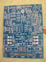
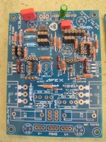
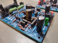
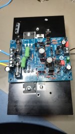
Board ready soldered.
No magic smoke.
input shorted with black wire- right of the pic.
it is heating up but runs into the current limiter of my lab psu. it is warming up without stabilization.
amp is running into the current limit of the psu. if i set 1,5A then it runs into it and the recommended 24V will never reached.
if i set the current limiter higher nothing happened for stabilization of the amp.
it is not working. no smoke. the Q1/Q2 get warm and the T14/15 neighbors warm up too - but nothing else.
psu is toggling from 3-12Volt and runs into CC limiter.
check´s:
All output transistor testes in the morning and the T14/T15 too. - okay
all resistor values checked - okay
all BJT To92 checked with DCA pro okay
no short between heat sink and any point of the output transistors - okay
GND2 i the schematic is connected to the PWRGND on the amp board. see pic
what i do not understand is the note what is written on the pcb?
extra wire from i/p GND to PSU GND
is this important for the my test too?
thanks
regards chris
Attachments
i found in the thread:
There is 1300mA auto bias circuit on AA14, can be set with change 0R22 resistors. Use +/-24V PSU for 20W.
auto bias to 1300mA
There is 1300mA auto bias circuit on AA14, can be set with change 0R22 resistors. Use +/-24V PSU for 20W.
auto bias to 1300mA
extra wire from i/p GND to PSU GND
There are 2 ground areas on the PCB:
a) power GND (dirty) - on the right hand side
b) input GND - on the left hand side
These 2 grounds are NOT connected to each other on PCB. The idea is to have TWO wires - from each of these grounds from the PCB, to the common ground point on the PSU.
Without these 2 grounds being connected, the amp will not work.
When they are connected this way (as opposed to being connected directly on the PCB), we are not mixing dirty and clean ground, which should minimize hum and distortions.
This is very nice and thoughtful PCB design. Kudos to Prasi.
Hi Minek
i did the test. i take an extra cable and put it at the minus terminal of the input terminal but the amp doesn't work again.
same behavior as wrote above-
could it be that the mica caps are to high?--> oscillation?
C10/ c11 22pF for the VAS transistors
or the feedback cap C8 is too high 33pF
kr
chris
If your amp is drawing > 1.5A , that would rather point to one of these simpler problems:
a) mistake/bad soldering
b) some transistors burnt
c) mistake in devices positioniong (e.g. E swapped with C on a transistor, diode backwards, etc..)
d) pcb traces shorted or missing
e) big caps in reversed polarity
Now, I noticed this is class A amp - what is the idle current supposed to be?
My remarks above apply to B/AB class amps...
'A' class amp can very well draw over 1.5A in normal working conditions....
It's very likely it draws 2-3 Amps. What is the rail voltage?
Edit. I see it's 24V rails. so it's likely it normally draws over 1.5 A
Alpha Nirvana amp I built was drawing 2.4A when idle.
Last edited:
Have you checked correctness of the PCB?
One strange thing I see, that SQUARE solder pad denotes 'COLLECTOR' for small transistors,
but for TO-126 transistors (BD139/BD140) SQUARE solder pad denotes 'EMITTER' instead.
Easy to miss it, and solder BDs in wrong way.
Edit: To add to confusion, for TO-220 transistors (T14/T15) square pad denotes the 'BASE'
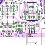
Judging from your photo and PCB analysis, your T9 is installed wrong way. Please verify schematic vs. PCB.
The image of T9 orientation on the PCB silkscreen might be incorrect.
T8 is correct. T9 should be oriented just like T8, not as mirror image.
I usually don't trust the silkscreen, especially on unverified PCB that no one else tried yet.
Verify the PCB vs schematic.
The image of T9 orientation on the PCB silkscreen might be incorrect.
T8 is correct. T9 should be oriented just like T8, not as mirror image.
I usually don't trust the silkscreen, especially on unverified PCB that no one else tried yet.
Verify the PCB vs schematic.
no i do not check the PCB correctness completly...maybe that is the reason...Have you checked correctness of the PCB?
One strange thing I see, that SQUARE solder pad denotes 'COLLECTOR' for small transistors,
but for TO-126 transistors (BD139/BD140) SQUARE solder pad denotes 'EMITTER' instead.
Easy to miss it, and solder BDs in wrong way.
Edit: To add to confusion, for TO-220 transistors (T14/T15) square pad denotes the 'BASE'
yes this is what i have checked. it is "always" marked the first (left to right) pin as "square" - this is not correct.
yes i will recheck the pcb first - orientation of the correct ECB according to schematic.
thanks for your time minek
kr
chris
i checked the PCB orientation to the schematic. i my opinion it is correct.
all diades are correct pcb vs. schematic.
TO-126 housing the Emitter is square.
TO-92 housing the collector is square.
T8 and T9 are correct implemented. these are 1381 3503
mhh... i need a pause...i am pissed ...i do not find the error
all diades are correct pcb vs. schematic.
TO-126 housing the Emitter is square.
TO-92 housing the collector is square.
T8 and T9 are correct implemented. these are 1381 3503
mhh... i need a pause...i am pissed ...i do not find the error
The copper side of pcb os correct - as far as T9 is concerned.
The base of T9 is on the right - when looking at the pcb images attached.
Base of T8 is also on the right.
Are you sure T9 is mounted correctly, with its base in correct position?
Judging from your photo, i thought the actual transistor T9 is facing wrong direction. Or can you attach close up photo of T9?
I see on the silkscreen, the image of T9 is wrong. If you followed what silkscreen suggests, then T9 is mounted wrong.
Do you see the mistake in the silkscreen?
- Home
- Amplifiers
- Solid State
- Apex AA14 Amp Class A 24V Supply