before i solder in i match all output transistor...so i expect that they are working therefore. with DCA pro it is not possible because its cant detected the equipment.
So they were ok BEFORE you started testing the amp?
And after that you didn't de-solder them to check?
And after that you didn't de-solder them to check?
i will optimize the cooling of the Q1 because i check that the output is massiv unsymmetrically at the beginning...maybe i was to afraid and switch off..
Q1 VCE starts at 34V and gets down...eat at the beginning 47,6WATT
Q2 starts at about 5V and gets up.
never the less it would be a big power up Thumb!!
Q1 VCE starts at 34V and gets down...eat at the beginning 47,6WATT
Q2 starts at about 5V and gets up.
never the less it would be a big power up Thumb!!
nope
it is still so...the Q! and Q2 are still keeping :
Q1 VCE starts at 34V and gets down...eat at the beginning 47,6WATT
Q2 starts at about 5V
i also try the cut out D7 D8 and and it si not working...i geuss that the ringing or what ever killed my Q2 maybe the Q1 too...will check...
it is still so...the Q! and Q2 are still keeping :
Q1 VCE starts at 34V and gets down...eat at the beginning 47,6WATT
Q2 starts at about 5V
i also try the cut out D7 D8 and and it si not working...i geuss that the ringing or what ever killed my Q2 maybe the Q1 too...will check...
Usually, if you have huge DC offset, it's either drivers or output devices mulfunctioning. In your case it seems like upper driver/output devices should be checked..

Hi again.
i de solder the Big Transistors Q1 and Q2 and measure them again with DMM and DCApro. i was surprised that the are working?!
so i thought that the transistor before push the Q1/Q2 strange and therefore i de solder them too. T15/14. but the test result was --> they are working (with DMM and DCApro)
aha...strange
okay i check the transistors before...VAS BD139/140...they or good and working.
what?!?
so actually status is: no Q1/Q2 and T14/T15 And D7/D8 is de soldered from PCB. so no heat is produced 😉
but i have still 22,6 V at the speakers + - GND Voltage!
Sin the next post i will show you my handwritten voltages.
i try to explain:
supply 24V. no really current is drawn by the amp.
no Q1/Q2 and T14/T15 And D7/D8 is de soldered from PCB
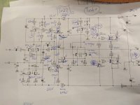
from left to right.
Differential input section
T3 is current source
VCE has 21,4V, VBE 0,6V
R4 560R drop is 626mV--> 1,1mA that is low but it is okay i think
rail is after R15 (minus 0,681V) 23,2V --okay
voltage drop on D12,D3 is 1,23V-okay
Voltage drop R7 22kR is 22V - okay
T1/ T5 are the differential input
T1 for the input signal
T5 for the feedback input from the speakers (R10 22k and C8 mica 33p )
T1 VCE is 23,1V , VBE is 0,6V --okay
T5 VCE 23,8V , VBE 8,7V...not okay
R5 (i dont know waht s therefore) is 22k and i have a drop of about 31mV
T2 and T4 is a current mirror and these are responsible to provide exact the same current in both "lines"of T1 and T5
R3 560 is 313mV -->550µA
R6 560 is 313mV -->550µA
this is exactly the same current/Voltage - fine...okay
D1 i do not know
R8 1k R i got 260mV ?
R10 Rf i got 22,6V (DC offset). where it get this voltage from??
supply 24V. no really current is drawn by the amp.
no Q1/Q2 and T14/T15 And D7/D8 is de soldered from PCB
from left to right.
Differential input section
T3 is current source
VCE has 21,4V, VBE 0,6V
R4 560R drop is 626mV--> 1,1mA that is low but it is okay i think
rail is after R15 (minus 0,681V) 23,2V --okay
voltage drop on D12,D3 is 1,23V-okay
Voltage drop R7 22kR is 22V - okay
T1/ T5 are the differential input
T1 for the input signal
T5 for the feedback input from the speakers (R10 22k and C8 mica 33p )
T1 VCE is 23,1V , VBE is 0,6V --okay
T5 VCE 23,8V , VBE 8,7V...not okay
R5 (i dont know waht s therefore) is 22k and i have a drop of about 31mV
T2 and T4 is a current mirror and these are responsible to provide exact the same current in both "lines"of T1 and T5
R3 560 is 313mV -->550µA
R6 560 is 313mV -->550µA
this is exactly the same current/Voltage - fine...okay
D1 i do not know
R8 1k R i got 260mV ?
R10 Rf i got 22,6V (DC offset). where it get this voltage from??
Attachments
This is weird. Without drivers and output devices, I think the only only way DC can get to the output is:
a) via D8/D7 - but they are also removed, right?
b) from T5 (damaged ?) - check voltage on the base of T5
c) via C12/C13 if they are damaged. Did you use capacitors from Ebay by any chance?
d) wrong grounding for the signal ground and damaged C6
a) via D8/D7 - but they are also removed, right?
b) from T5 (damaged ?) - check voltage on the base of T5
c) via C12/C13 if they are damaged. Did you use capacitors from Ebay by any chance?
d) wrong grounding for the signal ground and damaged C6
Last edited:
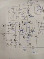
VAS:
T6 Darlington to T8 BD140, VBE 0,638V..okay
R13 220R 213mV---> 968µA - okay
R11 22k 21,4 Voltage drop --> 972µA...okay
T8 BD140 VBE is 1,65V..open..okay
T7 Darlington to T8 BD1139, VBE 0,622V..okay
R14 220R 213mV---> 968µA - okay
R12 22k 21,3 Voltage drop --> 968µA...okay
T8 BD139 VBE is 12,04V..open..okay
rail is after R14 (minus 0,459V) 23,5V --unsymmetrical but okay
Base T8 to T9 is 42,8V
a...yes soldered outThis is weird. Without drivers and output devices, I think the only only way DC can get the output is:
a) via D8/D7 - but they are also removed, right?
b) from T5 (damaged ?) - check voltage on the base of T5
c) via C12/C13 if they are damaged. Did you use check capacitors from Ebay by any chance?
d) wrong grounding for the signal ground and damaged C6
B is testet --okay
C no...source is digikey
D...have to check
Thanks
BTW i like your projects 😎
Check C12/C13. If lower one is shorted/leaking current - that would explain everything.
Check voltage between input ground and output ground, make sure they are both 0V.
Check voltage between input ground and output ground, make sure they are both 0V.
Of course one more reason could be E) mistakes on PCB
I tried to check the PCB, and I did't see anything wrong, but perhaps I missed something.
Or F) soldering problem - 2 soldering points soldered together (a short) somewhere...
Try to remove R10. If there is still DC on the output, it means PCB/soldering problems.
I tried to check the PCB, and I did't see anything wrong, but perhaps I missed something.
Or F) soldering problem - 2 soldering points soldered together (a short) somewhere...
Try to remove R10. If there is still DC on the output, it means PCB/soldering problems.
C6 de soldering is a nightmare...no space with my fingers....nice compact PCB layout 🤣
muse (UKZ) are fat and wires are fat
muse (UKZ) are fat and wires are fat
How C12 can be 0.9V ? That should be rail voltage +20V.
What PSU are you using? What current amp draws without output devices?
Is your positive rail voltage going to 0.9V on idle amp that doesn't even draw significant current?
I'm assuming LOW current, so the positive rail shouldn't sag, and Voltage on C12 should show +20V (or whatever your voltage supplies exactly are, little bit over 20V I guess).
Or C12 is damaged and shorting positive rail to the ground. You would need to desolder it and check.
Last edited:
R10 provides feedback signal back to the LTP input, and R8 divides that feedback voltage (ratio R10/R8). This ratio decides the gain of the amp.What is C6 and R8 for?
they should provide the correct base Voltage without passing DC or?
The lower R8, the higher gain. C6 makes sure gain is controlled only by AC signal, we don't want to amplify DC (if present in the output).
both have the supply voltage 23,9 V(24V) no leakageCheck C12/C13. If lower one is shorted/leaking current - that would explain everything.
Check voltage between input ground and output ground, make sure they are both 0V.
- Home
- Amplifiers
- Solid State
- Apex AA14 Amp Class A 24V Supply