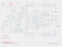
SA2016: using lateral mosfets EXC10N20 EXC10P20
... fixed minor errors
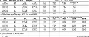
Noise output µV (wideband; bw 80k; bw 20k; A-weighted) with input shorted with 5k resistor (CCS and VAS BC327-40)
BR, Toni
... fixed minor errors
- nameing schema - SA2016 is the official name for this lateral MOSFET amplifier
- removed capacitor C16
Noise output µV (wideband; bw 80k; bw 20k; A-weighted) with input shorted with 5k resistor (CCS and VAS BC327-40)
Code:
IPS             wb      80k     20k     A-w
                µV      µV      µV      µV
-------------------------------------------
2SK170GR        160     86      42      32
BC337-40        168     92      47      35
BC550C 180 96 50 38Attachments
...Which Siglent did you buy?...
Hi Mogens,
SSA3021X - up to 2.1GHz. EMI kit is available too.
My old HP3585A is still a very good spectrum analyzer up to 40MHz and hopefully will have a long endurance.
SA2016: using lateral mosfets EXC10N20 EXC10P20
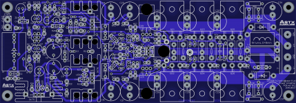
... new pcb's ordered ... hopefully now with no mask error ... 🙂
The design of the IPS has been adapted to be able to use cheap L-shape aluminium as a replacement for the sometimes hard to get small heatsinks SK75 and SK76.
... new pcb's ordered ... hopefully now with no mask error ... 🙂
The design of the IPS has been adapted to be able to use cheap L-shape aluminium as a replacement for the sometimes hard to get small heatsinks SK75 and SK76.
Attachments
Last edited:
SA2016: using lateral mosfets EXC10N20 EXC10P20
... some noise measurements using different transistors.
There are not really big differences viewable. The "no bandwidth limit" noise levels are dependent on the mains current quality! RF noise due to the many switching power supplies around because.
The noise betters less as 1dB if using BC327-40 or 2SK170GR instead of BC550C. THD levels are very similar. 2SK170 THD level with a lower degeneration resistor of 56R is very close to the BC types using 82R.
If bias is > 300mA per device the distortion residual is free from crossover artefacts at 20kHz full power.
IMHO this makes this amplifier very interesting: you can operate the amplifier with very low bias - 15mA per device - and you still get outstanding THD results. Also for the very important "first" watt!
BR, Toni
Attachments
Last edited:
by coincidence I installed 51r1 for the degeneration value ready for plugging in LSK170 input pair.............. 2SK170 THD level with a lower degeneration resistor of 56R is very close to the BC types using 82R.............i
by coincidence I installed 51r1 for the degeneration value ready for plugging in LSK170 input pair.
Very good! From simulation result there should be enough headroom regarding PM and GM.
Just tested with 2SK170GR Rdg 47R: no signs of instability. THD+N 20k/70W/8R 0.0035% bw 80k, 0.0052% no bw limit.
Slewrate > 100V sym.
BR, Toni
Last edited:
I am planning on running this beta test board on ±50Vdc.
Do you want the revised resistor values posted here?
I tried to make the currents from the higher voltage rails match those currents that would flow with 41Vdc rails.
Do you want the revised resistor values posted here?
I tried to make the currents from the higher voltage rails match those currents that would flow with 41Vdc rails.
Could you post a sch with test voltage at various nodes?
and a sch with design current values at various components?
and a sch with design current values at various components?
I am planning on running this beta test board on ±50Vdc.
Do you want the revised resistor values posted here?
I tried to make the currents from the higher voltage rails match those currents that would flow with 41Vdc rails.
Have tested the pcb with +/-50V maximum too. No problem so far with current values.
Feel free to post such a table here so we can simulate and compare with test results. Referred to schematic from post #1761.
Further on the "alternatives" plan: using double die Exicons with higher supply voltage ...
BR, Toni
The 3pair output stage using 100W mosFET devices is good for 150W of maximum output.
That is well in excess of what can be got into an 8ohms load from ±50Vdc
150W would be roughly the maximum output into a 4ohms load from a 30-0-30Vac transformer giving ~±42Vdc
Three pair of double die versions (250W) would more than double the potential maximum output power to around 370W.
370W into 4ohms is almost three times the current demand of a 100W into 8ohms amplifier. This would need an almightly PSU to meet the transient current demands.
Last edited:
To change from the ±41Vdc supply rails to using a 35-0-35Vac transformer giving ~±50Vdc you need to change six resistors
resistor ±41Vdc . ±50Vdc
R5 . . . . 22k . . . . 27k
R16 . . . 10k . . . . 13k
R29/30 . 12k . . . . 16k
R49/54 . 33k . . . . 42k?
For the protection locus you may have to also change R51/52
Why are these shown differently in the upper from the lower?
Have I missed any others that should be changed?
resistor ±41Vdc . ±50Vdc
R5 . . . . 22k . . . . 27k
R16 . . . 10k . . . . 13k
R29/30 . 12k . . . . 16k
R49/54 . 33k . . . . 42k?
For the protection locus you may have to also change R51/52
Why are these shown differently in the upper from the lower?
Have I missed any others that should be changed?
Last edited:
Hello folks,
I was wondering why you would not be using the double die version(ALF16P(N)20W) to start with 🙂 I know they are expensive.
John Curl was going on about Latfets needing too much extra drive voltage and intrinsic channel Rds losses. He can go camp out with Mr Self 🙂
I do agree that they should have the driver supply higher than the o/p device supply by about 10V.
I am using those latfets with OPC wire amp LME49830, it sounds/works nice for me. It makes the old Sansui G-7500 sing again. Used an old Pioneer SX-1050 PS. I get about 120W/ch into 8 ohm.
I measured the rise time to be ~600ns, fall around 650ns, which I do not think you can get from a bjt easilly? used a HP 3325A and a Tek DPO4034 for that measurement.
For HP fan noise, source/replace with a lower noise fan and/or or put it in a rack in which it was probably intended to go into.
Those fans make a wonderful noise when they are beating against each other = get a rack.
I think it would be nice to be able to use the over current detector to,
1) trigger a one shot and then drive a LED for visual
2) latch a speaker protection relay like Pioneer did in many designs.
3) Could be sent to a MCU to be processed
Just my ideas
Using a non regulated supply you find that while the supply rails sag, that both the input stage and the output sag together. This allows the input stage to drive the output FETs into saturation. They take a long time to come out of saturation.
If you keep the input stage from sagging, either by regulation, or very high capacitance after the RC, you find that the input stage can drive the output FETs even further into saturation. And take even longer to return to normal operation.
JLH published a Lateral mosFET amplifier where the output stage ran on supply rails that were much higher than those to feed the input stage. Many thought that JLH had made a mistake and got the rail voltages swapped by accident.
I wonder if he had experimented with what the amplifier sounded like when the output stage was driven into saturation on the loudest peaks compared to when the input stage that was incapable of saturating the output mosFETs.
Could there be a sound quality advantage when the output is very close to clipping, or actually clipping, where a very quick recovery from near saturation could be heard compared to a stage that takes a while to recover from the transient peak causing severe saturation?
I remember a few amplifier Designers have stated that all amplifiers sound the same when the amplifiers have identical frequency response and they are never asked to operate outside their "good behaviour" window. They only sound different when they misbehave and have to recover from that incident.
Last edited:
Dear Andrew,
thanks for update! Regarding output power you are right: only 8R load is allowed with those Exicons and ± 50V supply.
The SOA protection resistors (R49, R54) need not to be changed. Those are exactly fitted for use with ECX10[NP]20. Otherwise a complete redesign of all values is necessary. A quick SOA check running ±55V showed a enough safety margin for VAS, drivers and other transistors used here.
So effectively you need only to change those values as you recommend:
(my max. output power means: THD+N 20k below 0.01%!)
BR, Toni
thanks for update! Regarding output power you are right: only 8R load is allowed with those Exicons and ± 50V supply.
The SOA protection resistors (R49, R54) need not to be changed. Those are exactly fitted for use with ECX10[NP]20. Otherwise a complete redesign of all values is necessary. A quick SOA check running ±55V showed a enough safety margin for VAS, drivers and other transistors used here.
So effectively you need only to change those values as you recommend:
Code:
resistors  ±41Vdc    ±50Vdc
---------------------------
R5          22k       27k
R16         10k       13k
R29/30      12k       16k

transformers AC secondary
---------------------------
           2x30V     2x35V

max output power 8R
---------------------------
            78W      115W

max output power 4R
---------------------------
140W N/ABR, Toni
Dear Rick,
thanks for your input!
BR, Toni
thanks for your input!
... or use more output devices to lower current per device......
I do agree that they should have the driver supply higher than the o/p device supply by about 10V.
...
Unfortunately thats impossible for three reasons here:For HP fan noise, source/replace with a lower noise fan and/or or put it in a rack in which it was probably intended to go into.
- My electronic lab room is only 4+2.6m - no place for a big rack.
- Too heavy (> 50kg) to put it out of my rack and change parts inside
- don't want to change anything inside those old equipment as long as there is no problem... 😉
On my todo list for a SMD version.I think it would be nice to be able to use the over current detector to,
1) trigger a one shot and then drive a LED for visual
2) latch a speaker protection relay like Pioneer did in many designs.
3) Could be sent to a MCU to be processed
...
BR, Toni
the upper resistor (R49/54) feeds some of the power rail voltage into the protection transistor (prot Q) base.
This base voltage must never exceed the transistor turn on voltage, when the amplifier has no signal and no output current.
That rail voltage is effectively the IV's method of monitoring the V part of the protection locus. And the voltage across the emitter/source resistor is the way the IV generates the I part of IV.
Those two input signals feed into the prot Q base to either keep it turned off, or start to turn it on.
The harder one turns on prot Q, then the more that transistor sucks signal out of the signal feed into the output stage.
If one changes the supply rail voltage, then the base voltage on prot Q changes. The V resistor MUST be scaled to suit the supply rail voltage.
If you don't, then a very low supply rail will excessively delay the prot Q from turning on when needed to limit output.
Conversely, a very high supply rail voltage feeds too much current into prot Q and turns it on even though there is no output, or a very low output that should be considered a valid audio signal and that should pass without IV limiting.
Inadequate design of the IV that either does not limit, or limits valid signals, is not worth having. One must design the protection locus to suit the amplifier's loading conditions and that includes the supply rail voltage.
I was asked many times in an old Thread to redesign the IV for different amp builds. I refused because I knew that every apparent small change in operating conditions changed the IV component values. Instead I issued a few copies of the spreadsheet that showed the IV protection locus to allow the Builder to rescale the component values for their chosen operating conditions.
Last edited:
In principle you are right.
If you change one resistor in this dual slope IV limiter you need to redesign all others and the zeners too.
Stepping the supply voltage in simulation from 35V to 55V the currently implemented VI limiter behaves very well and the SOA limit curves overlap nearly at the same points so nothing to adapt here for the above supply voltage range and the used output transistors.
BR, Toni
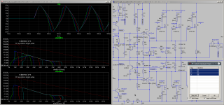
SA2016: using double die lateral mosfets ECW20N20 ECW20P20
Attached a SOA plot for the double die exicons with rail voltages stepped from 37V to 55 V. SOA lines overlap nearly exactly - mostly independent from supply voltage.🙂
BR, Toni
Attached a SOA plot for the double die exicons with rail voltages stepped from 37V to 55 V. SOA lines overlap nearly exactly - mostly independent from supply voltage.🙂
BR, Toni
Attachments
VAS current limit is different for positive and negative half wave and transistors Vbe differ a little. VAS current limit on positive half wave is about 40mA. CCS current limit on negative half wave is 12 mA. More base current for positive half wave is needed....
Why are these shown differently in the upper from the lower?
...
- Home
- Amplifiers
- Solid State
- 2stageEF high performance class AB power amp / 200W8R / 400W4R