Are You sure about the placing of the protecting zeners (ZD5-8)? The is no current limit once they open.
Sajti
The protecting zeners are only for a minimum ESD protection. 15V GateSource voltage would heavily exceed the maximum drain current. From datasheet: with Vgs of 6V you can reach the maximum 8A drain current ...
Current limit is done by the VI limiter - otherwise by fuse or holy smoke...
BR, Toni
If the limiter is too slow, or for some reason fails to operate, then the Zener will pull current through the driver transistor.
I would choose a much lower Zener voltage. Either 9V, or 12V, Zeners will allow plenty of transient current peaks if the load demands that.
You also need to check the earlier stages for an over-current condition if the IV triggers.
I would choose a much lower Zener voltage. Either 9V, or 12V, Zeners will allow plenty of transient current peaks if the load demands that.
You also need to check the earlier stages for an over-current condition if the IV triggers.
If the limiter is too slow, or for some reason fails to operate, then the Zener will pull current through the driver transistor.
And there is no limit for the current across the zeners. This is what I mentioned. The zener, or the emitter follower will fail, or maybe both...
You can solve this problem if You place the zener string between the VAS, and the driver...
Sajti
Yes, I understand.And there is no limit for the current across the zeners. This is what I mentioned. The zener, or the emitter follower will fail, or maybe both...
You can solve this problem if You place the zener string between the VAS, and the driver...
Sajti
I once suggested that the zener + protection resistor alone would make a good current limiter for the output mosFET.
I got jumped upon by a mosFET expert who took the time to explain what the mosFET would do when presented with an almost instant step change in output current with the Zener protection in place. Basically he said the mosFET would blow up because it exceeded it's deltaI/dt limits. (if I have remebered close to what he wrote).
As I said be4 the zeners are only for a minimum ESD protection. Normally ESD zener protection diodes should be connected directly at each mosfet gate to source.
The VI limiter is fast enough to protect the output devices. This protects also the drivers. SOA of drivers and VAS is safe during overload with full power output at 20 - 50mOhm load/short circuit. A simple VI limiter using only zeners wouldn't protect the amplifier if a short circuit condition occurs.
For best performance I remove the VI limiter completely! The VI limiter here is only an add on which can be tuned to best OPS protection at the cost of THD performance.
BR, Toni
if you refer to the schematic a view post be4:How do you determine the power rating of R46?
- simulation extremes ...
- physical testing...
- temperature control ...
R46 has to charge 2000uF to 41V. I had to think about what was limiting the inrush current, but it's not as demanding on a resistor as I thought at first.
Yes you are right! It would be more stress if the 41 Volt will be attached immediatly. In real life the big power supply need some 100s of ms to fully charge so no real stress here. Discharge on power off is much slower. Stress if VAS is overloaded is also marginal due to the VAS current limiter. Also the second 1000uf cap is decoupled by another 10R resistor. During testing I have had many situations where the current limiter of the regulated power supply immediatly shutted down the 42 V to zero Volt and never had a defektive R46 (0.6W).R46 has to charge 2000uF to 41V. I had to think about what was limiting the inrush current, but it's not as demanding on a resistor as I thought at first.
BR, toni
SA2016: using lateral mosfets EXC10N20 EXC10P20
This schematic looks now promising. All tests done with added VI limiter. Compensation and gate resistor values are more conservative to allow different small signal transistors.
Slew rate symmetrical > 100V/µs. Distortions marginal higher due to the added VI limiter.
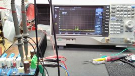
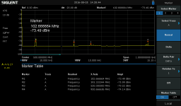
No more oscillations detected (total bias checked from 0.01A up to 1.8A). The attached spectrum shows only local FM radio stations, unknown 390MHz radio, 3 DVB-T television channels around 550MHz and 950MHz mobile.
Have tried to interchange small signal transistors. Fairchild BC337-40 and BC327-40 can be used as direct replacement. Technically 2N3904/2N3906 are working too (have a reverse pin direction compared to BC types.) but cannot be used on this PCB.
Surprise: overall noise is a little bit lower (1 - 1.5dB) if all BC3X7-40 are used.
All tested small signal transistors types are from fairchild.
Need to compare noise with original onsemi BC5X0C (which are now obsolete due to the merger with fairchildsemi).
Time to solder 2 PCBs for stereo tests ...
BR, Toni
This schematic looks now promising. All tests done with added VI limiter. Compensation and gate resistor values are more conservative to allow different small signal transistors.
Slew rate symmetrical > 100V/µs. Distortions marginal higher due to the added VI limiter.
No more oscillations detected (total bias checked from 0.01A up to 1.8A). The attached spectrum shows only local FM radio stations, unknown 390MHz radio, 3 DVB-T television channels around 550MHz and 950MHz mobile.
Have tried to interchange small signal transistors. Fairchild BC337-40 and BC327-40 can be used as direct replacement. Technically 2N3904/2N3906 are working too (have a reverse pin direction compared to BC types.) but cannot be used on this PCB.
Surprise: overall noise is a little bit lower (1 - 1.5dB) if all BC3X7-40 are used.
All tested small signal transistors types are from fairchild.
Need to compare noise with original onsemi BC5X0C (which are now obsolete due to the merger with fairchildsemi).
Time to solder 2 PCBs for stereo tests ...
BR, Toni
Attachments

Last edited:
This schematic looks now promising. Now with added VI limiter. Compensation and gate resistor values are more conservative to allow different small signal transistors.
Slew rate symmetrical > 100V/µs. Distortions marginal higher due to the added VI limiter.
No more oscillations detected (total bias checked from 0.01A up to 1.8A). The attached spectrum shows only local FM radio stations, unknown 390MHz radio, 3 DVB-T television channels around 550MHz and 950MHz mobile.
Have tried to interchange small signal transistors. Fairchild BC337-40 and BC327-40 can be used as direct replacement. Technically 2N3904/2N3906 are working too (have a reverse pin direction compared to BC types.) but cannot be used on this PCB.
Surprise: overall noise is a little bit lower (1 - 1.5dB) if all BC3X7-40 are used.
All tested small signal transistors types are from fairchild.
Need to compare noise with original onsemi BC5X0C (which are now obsolete due to the merger with fairchildsemi).
Time to solder 2 PCBs for stereo tests ...
BR, Toni
Toni glad to see your new amplifier functional.
Nice new spectrum analyzer!How you know what is at these frequences?
Thx! There exist official frequency tables ... 😉Toni glad to see your new amplifier functional.
Nice new spectrum analyzer!How you know what is at these frequences?
Is this the recommended sch for the PCBs that need a few mods to get working?This schematic looks now promising. All tests done with added VI limiter. Compensation and gate resistor values are more conservative to allow different small signal transistors.
Slew rate symmetrical > 100V/µs. Distortions marginal higher due to the added VI limiter.
No more oscillations detected (total bias checked from 0.01A up to 1.8A). The attached spectrum shows only local FM radio stations, unknown 390MHz radio, 3 DVB-T television channels around 550MHz and 950MHz mobile.
Have tried to interchange small signal transistors. Fairchild BC337-40 and BC327-40 can be used as direct replacement. Technically 2N3904/2N3906 are working too (have a reverse pin direction compared to BC types.) but cannot be used on this PCB.
Surprise: overall noise is a little bit lower (1 - 1.5dB) if all BC3X7-40 are used.
All tested small signal transistors types are from fairchild.
Need to compare noise with original onsemi BC5X0C (which are now obsolete due to the merger with fairchildsemi).
Time to solder 2 PCBs for stereo tests ...
BR, Toni
or is there a different sch for that PCB?
You can use this schematic for the "pcb need mod". The silk part numbers correspond with this schematic. bom will follow.Is this the recommended sch for the PCBs that need a few mods to get working?
or is there a different sch for that PCB?
BR, Toni
Can you explain in detail what and how you want it to be checked? thx, toniHow about with 5k source impedance?
was that spectrum to 1GHz done while the amplifier was outside an enclosure?............ All tests done ...........The attached spectrum shows only local FM radio stations, unknown 390MHz radio, 3 DVB-T television channels around 550MHz and 950MHz mobile...........
What filters were fitted to all the cables going into the enclosure?
Would the results change if RF fitering were added to all cables?
Shunt input to ground with a 5k resistor and measure output noise.
IIRC John Curl liked to use 2N2222 at 200uA because it worked better with high source impedances. Having low voltage noise is not very useful if your current noise is very high because of a volume pot. This is an advantage Jfet input amps have.
Also, absolute noise numbers for different input transistors will help selecting the right Rb for simulation models. (Or maybe you could just measure their noise directly out of circuit?)
No enclosure so RF is easy injected everywhere during tests. Amplifier itself seems to be imune to RF. Mobile or WLAN signals do not affect the amplifiers stability and/or distortion values.was that spectrum to 1GHz done while the amplifier was outside an enclosure?
What filters were fitted to all the cables going into the enclosure?
Would the results change if RF fitering were added to all cables?
- Home
- Amplifiers
- Solid State
- 2stageEF high performance class AB power amp / 200W8R / 400W4R