What's brand/label of emitter resistors? Look like metal elements/plate type (RGC 5, MPC74, BPR58). I like this type, it's small.
And i think you can change CCS, by 2 Q, it's better.
And i think you can change CCS, by 2 Q, it's better.
After changing the current mirror, what will greatly reduce the VAS distortion is to put R17 across the B-E of Q11, instead of including the degeneration. Then replace Q9 with a fast high-gain transistor. OStripper uses the KSA992. If the voltage were lower I'd use a BC560C.
The 22pF bridge cap on the TPC may not help stability and circumvents the improvement of TPC. I would suggest you try removing it.
The ratio of C8 and C10 could be better. For TPC you want C10 to be around 5 times C8. for less input stage loading you can reference R16 to Q11's emitter. R16 should not go to ground, else you are causing PSRR.
I get 390p, 82p and 3.9k as new values for C8, C10 and R16 respectively for the same corner frequency and miller capacitance after eliminating the bridge cap.
I think the above changes as well as the CM may greatly reduce THD, although it seems you'll only be able to see the effect in simulation.
Dear keantoken,
thanks for analyzing/answering.
To not confuse our readers we should not mix component numbers from schematics from post #1 with component numbers from asc file. The numbering scheme is different.
So following component numbers refer to schematic pictures from post#1.
The TPC values where first simulated and after many hours of fighting against oscillations manually selected.
R16: ist connected to silent ground which is OK
If I correctly remind increasing C10 and we get asymmetric slew rate...
Give me some time - have to simulate/test now.
Big THD improovement
Dear Harry,
currently simulated: C8/C9 junction to Q2 Emitter - heavy oscillations.
But keeping C9 in place and only left junction of C8 to Q2 emitter ROCKS!
THD20k@200W@8R betters from 0.0033% to 0.0017% !
THD100k@200W@8R betters from 0.054% to 0.019% !
(Q9 has been replaced by a KSA992).
My solder iron is currently heating up ...
(NOTE: part numbers refer to schematic pictures from post #1)
This is not correct. To get the best PSRR, R16 should go to ground and the C8/C9 junction should go to Q2 emitter instead of collector. Note that this altered connection will probably require compensation to the minor loop. See section 3.4 and addendum of my paper on two-pole compensation.
forgot to say thank you for the link to your paper!
BR, Toni
What's brand/label of emitter resistors? Look like metal elements/plate type (RGC 5, MPC74, BPR58). I like this type, it's small.
And i think you can change CCS, by 2 Q, it's better.
Indeed they are MPC74. Very low inductance.
Have to investigate "CCS, by 2 Q".
BR, Toni
forgot to say thank you for the link to your paper!
BR, Toni
You are welcome! Thanks also are due to the AES for allowing me to freely distribute the paper 🙂
Dear Harry,
currently simulated: C8/C9 junction to Q2 Emitter - heavy oscillations.
But keeping C9 in place and only left junction of C8 to Q2 emitter ROCKS!
THD20k@200W@8R betters from 0.0033% to 0.0017% !
THD100k@200W@8R betters from 0.054% to 0.019% !
(Q9 has been replaced by a KSA992).
My solder iron is currently heating up ...
(NOTE: part numbers refer to schematic pictures from post #1)
Real life is often very different from simulation. Here are the first measurements (all THD20K@200W@8R; bandwidth 80kHz):
- Q9 replaced by KSA992: THD dropped from 0.0039 %to 0.0036%
- left leg C8 to Q2-emitter: THD dropped from 0.0036% to 0.0030%
This is a no go. Needs more investigation. Next version amplifier!
Next step try to improve current mirror: replaced 2N5401 with new matched BC560C. Distortions increased to 0.0040% but a little bit lower HF noise. Degenerate R7 and R10 by 220R shows now THD 0.0036% and lower HF noise. Keeping it.
Thats for now. Many hours testing and results are 3 - 4 ppm THD and a litlle better noise figure.
As i have another unmodified module the next step is to compare the sound ...
BR, Toni
But transient analysis showed the problems: moving C8 leg to Q2-emitter worsens stability. The transient edges are showing little staircase patterns - a sign for too less compensation/oscillation somewhere.
Sounds like instability of the minor loop. See the addendum to my paper.
I note that in post #1 you include a loop gain bode plot performed with a tian probe so you should be able to fairly easily perform the sims required to assess stability of the minor loop (I find it's easiest to create a duplicate schematic because the loop gain probe has to be inserted elsewhere and extra components are required to disable the major loop). I assume you are also observing the effects that the changes you make have on the major feedback loop?
To get high PSRR you will need both C8 and C9 to go to Q2 emitter. PSRR is also easy to simulate.
Astx, the 22p bridge capacitor may be needed because the output stage needs to see a capacitive source impedance. Try removing it and hanging a cap from the VAS output to ground. I'm not sure how large this cap should be. It may need a 15R or so series resistor, when the VAS degeneration is taken into account. I suggest trying values between 100p-1n. I would suggest using a small 100R trimmer in series because the correct values can be very important. In any case, to give a capacitive source impedance we don't need to emulate it with the VAS, which conducts OPS distortion unnecessarily into the IPS.
The suggestions I gave work well to mitigate their respective distortion mechanisms, but it is easy for Miller capacitance to dominate, in addition to other things.
The suggestions I gave work well to mitigate their respective distortion mechanisms, but it is easy for Miller capacitance to dominate, in addition to other things.
Astx, the 22p bridge capacitor may be needed because the output stage needs to see a capacitive source impedance. Try removing it and hanging a cap from the VAS output to ground. I'm not sure how large this cap should be. It may need a 15R or so series resistor, when the VAS degeneration is taken into account. I suggest trying values between 100p-1n. I would suggest using a small 100R trimmer in series because the correct values can be very important. In any case, to give a capacitive source impedance we don't need to emulate it with the VAS, which conducts OPS distortion unnecessarily into the IPS.
The suggestions I gave work well to mitigate their respective distortion mechanisms, but it is easy for Miller capacitance to dominate, in addition to other things.
Dear Keantoken,
thank you for the tip. Your variant is working in simulation:
removed 22p, C8 to emitter of Q9, added VAS cap+resistor. Beginning with 1n + 15R it starts to be stable. But now the SOA of the Q11 / 2SA1930 will be more and more violated due to the added capacitive load. 🙁
So we would have to change the VAS driver ...
Another problem arises: my testing equipment has reached the limits.
If you compare the last THD/power plot with the analyzer reference plot...
0.0034 THD20k@80kHz Bw @ 200W @ 8R is for the moment a very acceptable value - if the amplifier also sounds good 😉
Btw: 150W@8R distortion level is 0.0023%
The next days some new driver BJT's are coming and I plan to simulating/retest all findings.
By increasing or lowering the 15R you may be able to lower the 1n cap. These values depend on OPS parasitics, so can take some tuning. Most importantly, does this change decrease distortion?
Would the 2SC4793/A1830 be more suited for your VAS? They have SOA advantages compared to the C5171/A1930.
Would the 2SC4793/A1830 be more suited for your VAS? They have SOA advantages compared to the C5171/A1930.
Sounds like instability of the minor loop. See the addendum to my paper.
I note that in post #1 you include a loop gain bode plot performed with a tian probe so you should be able to fairly easily perform the sims required to assess stability of the minor loop (I find it's easiest to create a duplicate schematic because the loop gain probe has to be inserted elsewhere and extra components are required to disable the major loop). I assume you are also observing the effects that the changes you make have on the major feedback loop?
To get high PSRR you will need both C8 and C9 to go to Q2 emitter. PSRR is also easy to simulate.
Dear Harry
thank you for answering. There is so many to learn how to measure amplifier stability correctly. The Tianprobe in the NFB loop is only one test. If you have some hints where to find the error in the minor loop which is only visible in real world design and not reproducable in simulation? Where to set which probe type in simulation would be helpful.
I have added this test to the simulation.
; OPEN LOOP GAIN STABILITY TEST
; add this trace to your plot area:
; -V(x)/V(inpneg)
.param prb 0
V3 x inpneg AC 1
V4 gnd inppos DC 0
.ac dec 30 1Hz 100Meg
.meas ac pmargin find (V(x)/V(inpneg)) when mag(V(x)/V(inpneg))=1.00V cross=1
.meas ac gmargin find mag(V(x)/V(inpneg)) when ph(V(x)/V(inpneg))=0 cross=1
.meas ac db20k find (V(x)/V(inpneg)) when freq=20000 cross=1
.param Rswitch= 1T
Don't know if this simple test is correct to measure OLG - it shows "-220" degree which is unstable. If all compensation is reverted to first schematic it shows "-133" degree which would be a comfortable 47 degree phase margin or in other words stable. This simple test helped me to get the amplifier rock solid stable and seems to explain why the compensation variant can be only stable if we set the gain relatively high.; add this trace to your plot area:
; -V(x)/V(inpneg)
.param prb 0
V3 x inpneg AC 1
V4 gnd inppos DC 0
.ac dec 30 1Hz 100Meg
.meas ac pmargin find (V(x)/V(inpneg)) when mag(V(x)/V(inpneg))=1.00V cross=1
.meas ac gmargin find mag(V(x)/V(inpneg)) when ph(V(x)/V(inpneg))=0 cross=1
.meas ac db20k find (V(x)/V(inpneg)) when freq=20000 cross=1
.param Rswitch= 1T
Am I wrong?
BR, Toni
By increasing or lowering the 15R you may be able to lower the 1n cap. These values depend on OPS parasitics, so can take some tuning. Most importantly, does this change decrease distortion?
Would the 2SC4793/A1830 be more suited for your VAS? They have SOA advantages compared to the C5171/A1930.
It helped to get harry's variant without the C9/22p cap stable - and helped therefore indirectly to improve distortion.
Think 2SC4793/A1830 bjt variants may help to get more out of the current design. The 2SC5171/2SA1930 are very good (and unfortunately discontinued) but have a really bad SOA.
Safety and stability is more important as a few ppm less THD ...
BR, Toni
Last edited:
Nice lab 😉 .
Yesterday made some measurements with R17=150R.
Most of the H2/H3 is produced from the analyzer oscillator output itself.
Load 8R, 200W, 20kHz.
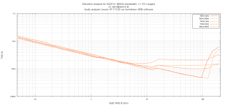
Distortion analysis for current improvements
See attached distortion plot for SA2013
At very high power levels (100W - 200W) the THD values for 20Hz and 200Hz are not representative as the used regulated laboratory power supplies started activating the current limiter ...
(need better test power supplies. 😉)
Can someone compare these results with other real life amplifiers out there to get a feeling in which category the 2stageEF may be now playing?
Attachments
Last edited:
Hi Astx,
What do you mean by category ?
kind regards,
Harrison.
What do you mean by category ?
kind regards,
Harrison.
See attached distortion plot for SA2013
At very high power levels (100W - 200W) the THD values for 20Hz and 200Hz are not representative as the used regulated laboratory power supplies started activating the current limiter ...
(need better test power supplies. 😉)
Can someone compare these results with other real life amplifiers out there to get a feeling in which category the 2stageEF may be now playing?
an invitation
Hi Astx,
Would you be willing to carry out comparison tests between your amplifier and http://www.diyaudio.com/forums/solid-state/219354-1diffqc-amplifier.html . As we explore the contribution of THD and PSRR in the listening experience ?
kind regards,
Harrison.
Hi Astx,
Would you be willing to carry out comparison tests between your amplifier and http://www.diyaudio.com/forums/solid-state/219354-1diffqc-amplifier.html . As we explore the contribution of THD and PSRR in the listening experience ?
kind regards,
Harrison.
Hi Astx,
What do you mean by category ?
kind regards,
Harrison.
category something like:
- cheap consumer amplifier
- ...
Hi Astx,
Would you be willing to carry out comparison tests between your amplifier and http://www.diyaudio.com/forums/solid-state/219354-1diffqc-amplifier.html . As we explore the contribution of THD and PSRR in the listening experience ?
kind regards,
Harrison.
Can you refine your Ideas?
BR, Toni
- Home
- Amplifiers
- Solid State
- 2stageEF high performance class AB power amp / 200W8R / 400W4R