Reduced to the max. What I do not understand: single or doublesided to fab there is no big difference in price.
The diameter of the hole for the bias transistor should be about 7-8mm. This helps during mount a lot.
You need two zobels: one on the board (!), the other directly at case speaker output.
Have fun, Toni
The diameter of the hole for the bias transistor should be about 7-8mm. This helps during mount a lot.
You need two zobels: one on the board (!), the other directly at case speaker output.
Have fun, Toni

Dear Toni
Reason I'm going single layer for larger project is because my local PCB supplier doesn't support multilayer via/pads, I have to short both layers on each parts by myself in that case.
There are professional manufacturer here but they are cost efficient with bulk quantity.
Hope you understand.
As for the design, that was just the first draft I will re-add the "opt" components in next designs and will keep zobel and use both zobel.
However the trickiest part will be finding good hfe matching output transistors here. I do have some matched MJL4302/MJL4281 what do you think of those?
You can't replace the recommended output transistors TTC5200/TTA1943 using other types without redesign of the TMC compensation. The MJL4302/MJL4281 will oscillate like hell in the SA2014.
No jig needed for the doublesided variant. If money is the problem and not the spare time: print on paper and glue on cardboard, cut out the windows. Bend the transistor legs, insert them on the circuit board, adjust the transistors on the prepared cardboard and attach them temporarily with adhesive tape. Solder carefully - first only the middle pin. unnecessary to say, the cardboard should be perfectly plain. 😆
With due respect, Toni, in comparison with a properly designed, two sided PCB this appears to bei a, erm, crudge ;-).
Best regards!
Best regards!
Unfortunately you are so right ... 😎
Of course I can't give support for single sided pcb's or foreign pcb designs which haven't materialized on my work- and testbench... sometimes a few extra pF or nH or a bad current loop on a pcb design can ruin the best circuit design...
Of course I can't give support for single sided pcb's or foreign pcb designs which haven't materialized on my work- and testbench... sometimes a few extra pF or nH or a bad current loop on a pcb design can ruin the best circuit design...
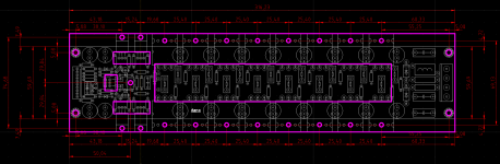
BTW: The NGFB point needs to be connected directly at output coil. The shown feedback connection is bad design. Have a look at the original 2sided PCB - there is a small trace from output coil to the INPUT/VAS stage connector.Single sided (untested) version of SA2014 output stage.
Tried to do with as less jumpers as possible, it's only 2 jumpers now because of the removal of "opt" components else there'd be much more.
Need to do a lot of optimisations to the layout before sending to fab.
Thinking about moving zobel network part to speaker protection board.
Any suggestions are always welcome 😀
Nice amp, easily does 100V/us, however 8 output pairs are risky and have a slim safety margin against oscillation without compensation adjustment , probably miller is better for fewer output pairs and the VI limiting mustn't be omitted, maybe do a custom redesign for him to fit his setupA jig made from wood or plastic could help solder the parts ...
Preliminary results show the SA2013 has the lowest IMD in the test set 👏, what speakers are you using? This may make harsh recordings sound harsh
Hi Tony,
Is the LTP+VAS of SA2014 same with SA2021-NCH?
If yes, can I use SA2014 front-end board to SA2021-NCH?
Do you have plan in future to make break-out output board for SA2021-NCH because it's a bit too long.
Just asking🙂
Is the LTP+VAS of SA2014 same with SA2021-NCH?
If yes, can I use SA2014 front-end board to SA2021-NCH?
Do you have plan in future to make break-out output board for SA2021-NCH because it's a bit too long.
Just asking🙂
Theoretically the frontend of SA2014 could be used for SA2021-NCH. IMHO: a high-end project deserves a high-end pcb.
Gerbers for this amplifier are currently not available.
Gerbers for this amplifier are currently not available.
Hello friends, and all the best in the new year to all of us...
I'm slowly finishing my SA2015 V-Mos for 4-channel bi-amping, and I have a question for @astx
1, Can I use thin KERAFOL under power mosfets? Can oscillations occur through the thin KERAFOL pad?
2, Or use a thicker ceramic pad just to be safe?

I'm slowly finishing my SA2015 V-Mos for 4-channel bi-amping, and I have a question for @astx
1, Can I use thin KERAFOL under power mosfets? Can oscillations occur through the thin KERAFOL pad?
2, Or use a thicker ceramic pad just to be safe?
Best 2025 to you all!
I have used kerafol for all my amplifiers. The mosfets stay cool and your fingers are clean!
Have fun, Toni
I have used kerafol for all my amplifiers. The mosfets stay cool and your fingers are clean!
Have fun, Toni
Using TTC5200 and TTA1943 providing such output power levels we need so much devices to fulfill SOA requirements under any type of reactive load.
Using other and less output devices is possible but the amplifier may behave completely different. E.g.: I have a duplicate of the output stage using MJW3281A and MJW1302A. This one is harder to get stable and simulation showed me why...
I would like to start by thanking you, Toni and the community for the design and all the related resources for this project. After going through this thread I decided to build SA2014, so I went ahead and fabricated the boards.
I have two questions regarding the alternate output device's stability in post#889
Q1, I wish to use NJW0302G and NJW0281G because I already have them from previous project and don't want to buy new devices (mainly due to budget). Do you think I will run into stability issues?
Q2, I don't have driver transistors (2SC4793 & 2SA1837) can I use MJE15032 & MJE15033 in there place? I had ordered TTC011B & TTA006B but I got TTA006B but need to wait for TTC011B since it is not in stock.
Best Regards,
Arshad.
Dear Arshad,
thanks for the kind words!
Ad Q1: using NJW0302G and NJW0281G would require a redesign of the VAS/Output stage. I never got it stable using > 4 pairs MJW3281A and MJW1302A. The TTC5200 and TTA1943 are inexpensive and 8 pairs guarantee you lowest THD and highest reliability.
Ad Q2: Using MJE15032 & MJE15033 is a no go. They have to low hFe and are too slow. You need the high gain of 2SC4793 & 2SA1837. Note: It's a 2 stage EF output.
TTC011B & TTA006B are on stock @ mouser india. Note: the pinout orientation is different from the 2SC4793 & 2SA1837!
BR, Toni
- Home
- Amplifiers
- Solid State
- 2stageEF high performance class AB power amp / 200W8R / 400W4R