...
I hope that my SA 2015 will be very happy in this house soon.
I'm sure it will!🙂
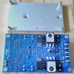
heatspreader - to be mounted with 2 x M5 on big heatsink.
Looks very nice!
Quick question: why do you use a heat spreader? Isn't it better to mount the PCB directly to the heatsink? This way there is a temp junction less.
Looks very nice!
Quick question: why do you use a heat spreader? Isn't it better to mount the PCB directly to the heatsink? This way there is a temp junction less.
Thanks! Of course they are not really necessary but I use it because:
- heatspreader 10mm thick is manufactured at a CNC fab including M3 screw tapping which I hate. Making M3 taps soon becomes a night mare and your heatsink is afterwards unusable
- heatspreader only requires 2 x M5 tap which can easier be done by yourself
- you can use even multiple main heatsinks with lower base plate thickness. E.g. "Modu pessante dissipante" case comes with 2x heatsinks on each side.
- you could use heat pipes if you need many modules in one case
- it looks cool
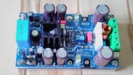
A new member in the family!... alive out of the box.
- VAS diode and over current protection in situ
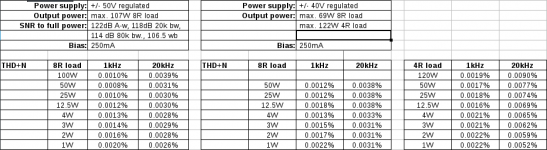
- THD20k 100W@8R: 0.0045% (80k bw.)
BR, Toni
Really nice work again.

SA2015: using vertical mosfets IXTH80N20L and IXTH48P20P
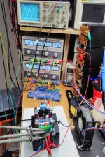
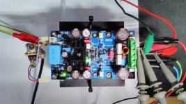
Some measurements, see attached picture.
Driving 4R load with +/-50V supply is not specified.
The amplifier modules have been soldered with components out of the box. No matching of any component values have been done. For LTP and current mirrors I have used transistors from same lot.
VAS diode and dual slope current limiter are in situ.
The distortion analyzers (Panasonic/Levear VP-7723D) sweetspot wasn't optimized during testing of lower power modes (1 - 4W). So it is expected this circuit to have better distortion figures in the "first watt" range as shown in the measurements table.
BR, Toni
Attachments
Last edited:
Some measurements, see attached picture...
Hi Toni
Nice to see measurements, and nice measurements, my compliments😉
How do the measured results compare with the simulations?
Do I need to tweak the models?
Best wishes
David
The results confirm D.Self's "Load Invariant" philosophy.
The higher current load increases the distortion. In most cases @ the same power into the 4ohms non reactive load the distortions are roughly doubled.
To me it is slightly surprising that the higher supply rail voltages significantly reduce distortions into the 8ohms non reactive load.
Is there an explanation of why this is so?
Yes.To me it is slightly surprising that the higher supply rail voltages significantly reduce distortions into the 8ohms non reactive load.
Is there an explanation of why this is so?
At HF, one of the biggest THD factors is wonky Cob of the VAS. Cob is reduced at higher Vce and hence, also its wonkiness, for a given output voltage.
Last edited:
Hi Toni
Nice to see measurements, and nice measurements, my compliments😉
How do the measured results compare with the simulations?
Do I need to tweak the models?
...
Dear David,
thanks!
IMHO your models are very good. The real life measurement result deltas are the same compared to all other simulated SA20xx variants.
Hopefully you will release the IXYS models as V1.0 for the DIYaudio community ... 🙂
... and provide us more transistor models in the near future ... 😀
Many thanks goes to you bringing the IXYS mosfets to my mind. Really nice parts!
BR, Toni
Maybe because I don't fully undertstand the AC theory of a complex amplifier, I thought that the Cdom version of the VAS with lots of it's own HF feedback and that there is another gob of global feedback that the VAS Cob generated distortion was reduced to nearly unmeasurable levels.Yes.
At HF, one of the biggest THD factors is wonky Cob of the VAS. Cob is reduced at higher Vce and hence, also its wonkiness, for a given output voltage.
But that is not what ASTX has measured.
He has ~38ppm @ 40Vdc reducing to ~30ppm @ 50Vdc. 12.5W into 8r0 @ 20kHz
That's high levels of distortion for a nearly "Blameless" style of topology.
And that is why I was surprised.
Last edited:
...
He has ~38ppm @ 40Vdc reducing to ~30ppm @ 50Vdc. 12.5W into 8r0 @ 20kHz
That's high levels of distortion for a nearly "Blameless" style of topology.
...
Don't forget: these values are with VAS diode and dual slope current limiter in situ. Remove those parts and you can measure "blameless" distortion values.
BR, Toni
Is the limiter starting to limit at your test voltages?
Have you tried slowing down the limiter so that it does not respond to very fast currents?
Have you tried slowing down the limiter so that it does not respond to very fast currents?
is that measureable in a sim that looks at that current?A dual slope limiter always injects some error currents from rails...
BR, Toni
What if the applied Vbe were only 400mV? what if the applied Vbe were reduced to 350mV?
Does that show as different in the sim?
I can imagine that the protection transistor with a Vbe exceeding 500mV would start passing some current and starting to steal the base current from the output stage. But the protection transistor should not be seeing base emitter voltage as high as that when the protection is not being activated.
Last edited:
You can examine those error currents (stealing base currents from drivers) using the simulation.
The limiter transistors need to be biased relatively high so always some leakage currents flow. A slow down capacitor (22pF) is already installed. IMHO if you make it too big you have 2 problems which increase also THD:
In post # 2174 I have measured the THD+N20k@60W@8R with 0.0018% when VAS diode and current limiter are not installed. So one can decide himself which level of protection to use ...
BR, Toni
The limiter transistors need to be biased relatively high so always some leakage currents flow. A slow down capacitor (22pF) is already installed. IMHO if you make it too big you have 2 problems which increase also THD:
- higher nonlinear capacitance from driver base to emitter via current limiter diode and current limiter transistor/resistor divider.
- too slow reaction on high current transients on short circuit
In post # 2174 I have measured the THD+N20k@60W@8R with 0.0018% when VAS diode and current limiter are not installed. So one can decide himself which level of protection to use ...
BR, Toni
...Hopefully you will release the IXYS models as V1.0 for the DIYaudio community ... 🙂
OK😉 now we have some confirmed data, ready for beta release, anyone wants the models just ask and I will email them.
I may talk to IXYS before full public release.
... and provide us more transistor models in the near future...
As you wish🙂 Which ones do you want?
...the IXYS mosfets to my mind. Really nice parts!
Yes, they looked nice, really pleased this has worked so well.
Best wishes
David
Hello,
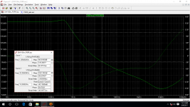
Has anyone tried the PSRR directives of astx amp to a different schematic? I tried it on my schematic but not sure if the plot shows the correct figure. I do not know how to derive the Rpsrrp & Rpsrrn values, input source is a typical AC sine wave with an amplitude of 0.6v at 1KHz freq. It roughly outputs 50w of power. Shown is my schematic and the graph plot with the cursor set at 1KHz & 20KHz respectively. PSRR test is + rail only.
Sorry off topic but got a post approval from Sir Toni.
Sa muli,
Albert
Attachments

...
I do not know how to derive the Rpsrrp & Rpsrrn values, input source is a typical AC sine wave with an amplitude of 0.6v at 1KHz freq.
...
Rpsrrp and Rpsrrn are switches:
- value 1T = switch open
- value 1n = switch closed
"PWRGRND" is not viewable on picture - is it low ohmic connected to ground?
BR, Toni
- Home
- Amplifiers
- Solid State
- 2stageEF high performance class AB power amp / 200W8R / 400W4R