The stoppers should be as close the the device pin as possible for greatest effect. As far away as they are on the layout they might not be very effective. Most reliable way would be a scope. I'm not really well versed on testing that. One issue is that it won't always oscillate, but if there is the right rf on the area it can start. Or with a particular signal. George would probabpy be really helpful with this aspect given his former day job
As far as the Schade resistors, it's the amount of feedback is important. A lower value of the resistor may be appropriate given the load the active device needs for a particular op point, but you would want to keep track of the amount of feedback to keep the curves where you want. I think I might have misunderstood your post and thought you might be lowering the feedback chasing the bandwidth. One thing to test after tweaking the resistors is to rerun the curves to see if they still look the way you want. And to be fair, I'm certainly not an expert. And the solid state devices are a bit out of my comfort zone, but the operation of Schade feedback should still apply.
Yeah, I try to wire mine as close to the gate pin as possible. On the PCB, there has to be some clearance around the device for heatsinks, and then it is just a short distance to the resistor. I'll take another look.
Also, with regard to square waves, isn't bandwidth a primary determinant of clean square waves? The higher the frequency you can reproduce, the faster the rise and fall times. That's what I know from my limited knowledge of circuit theory. I'm sure there is more to it.
Also, with regard to square waves, isn't bandwidth a primary determinant of clean square waves? The higher the frequency you can reproduce, the faster the rise and fall times. That's what I know from my limited knowledge of circuit theory. I'm sure there is more to it.
The only components connected to the gate of the gain mosfet are resistors. Each has a value larger than the usual stopper. As long as they are both close to the gate pin of the gain fet, they ARE the stoppers.The bottommost FET has a stopper. The top two form the CCS and have 220 ohm stoppers. The middle, gain, FET has no stopper. Does it need one?
There is a capacitance between the gate pin and both the source and drain pin of any mosfet, or even a tube or j-fet. This capacitance changes with the applied voltage, particularly in a mosfet. Even a tube sees a Voltage Varying Capacitance effect due to the modulation of its space charge, but the space charge is lossy, so this is a minor effect. The RC pole formed between the gate capacitance and the feedback resistors forms a low pass filter, rolling off the feedback at some HF point. This can cause a peaking in the HF response as the feedback is reduced with increasing frequency. Adding a small capacitance across the feedback resistor will roll off the HF response because of this.The purpose of the schade feedback is for triode like behavior and linearity at audio frequencies. It makes sense that the feedback will limit the bandwidth, but with that limit, the design would hopefully have better audio quality.
Most of my experiments have been done with vacuum tube output stages where the plate voltages can exceed 1KV under overdriven conditions into a reactive load so the feedback resistor is often quite large in value and made of several resistors in series to avoid flashover. The cap may not be needed in solid state preamp / VAS circuits due to the lower resistor values.
One issue is that it won't always oscillate, but if there is the right rf on the area it can start. Or with a particular signal. George would probabpy be really helpful with this aspect given his former day job
Also, with regard to square waves, isn't bandwidth a primary determinant of clean square waves? The higher the frequency you can reproduce, the faster the rise and fall times.
The overall bandwidth, and flatness of the HF response in the frequencies above the frequency of the test tone (10KHz in the usual case) affects the square wave reproduction. There are two things at play here that can conflict. The steady state small signal response of the circuit may be quite stable and no oscillation may be seen. However the gate capacitance of the active gain fet changes dynamically with the applied signal. It goes up dramatically as the voltage across the fet approaches zero. Most circuits involving tubes and mosfets that I have built for the last 20 years will emit a short burst of oscillation at the point where the mosfet enters or leaves saturation or cutoff. Obviously, a pure class A circuit of this type shouldn't go there, but sometimes a dumm blonde will plug in his guitar preamp and "set the controls for the heart of the sun" just to see what happens. Why? because someone somewhere will build one of my amps and do something similar, or even crazier. Seriously, it took me several years before I realized that using mosfets to directly drive the grid of a high Gm vacuum tube works best if the fet is always conducting and always has tens of volts across it even when the tube it is driving is cut off in a push pull amp.
In applications where there is an inductive load that has a HF roll off like an OPT, I try to limit the HF response of the gain stages. MHz of bandwidth is not needed for audio, and does have drawbacks. Since there is virtually zero musical need for 10 KHz square waves, I tens to test with a 5 KHz square wave, especially when large OPT's are involved.I think bandwidth > 100 khz is more than adequate. Also, I strongly suspect if you build that layout with anywhere near the bandwidth you describe you will have massive oscillations.
I have a breadboard of this circuit about half finished sitting in a dark corner of my bench. Once some other priorities are out of the way it will see completion, and lots of testing. The "last new tube amp design" I want to conquer is the high efficiency tube amp I started for the 2008 magazine article mentioned in post #63. Some big tubes in a cathode follower circuit will be feeding some 600 ohm OPT's that recently arrived from Poland. There are also some big SiC fets in a Fedex truck somewhere between Mouser and me that might just find their way into that tube socket too.
Last edited:

It is like drinking from a hose, George. There is so much info in that post.
Thanks! That's cleared up.The only components connected to the gate of the gain mosfet are resistors. Each has a value larger than the usual stopper. As long as they are both close to the gate pin of the gain fet, they ARE the stoppers.
I did measure this today. Will post the results. Very helpful to read your explanation.There is a capacitance between the gate pin and both the source and drain pin of any mosfet, or even a tube or j-fet. This capacitance changes with the applied voltage, particularly in a mosfet. Even a tube sees a Voltage Varying Capacitance effect due to the modulation of its space charge, but the space charge is lossy, so this is a minor effect. The RC pole formed between the gate capacitance and the feedback resistors forms a low pass filter, rolling off the feedback at some HF point. This can cause a peaking in the HF response as the feedback is reduced with increasing frequency. Adding a small capacitance across the feedback resistor will roll off the HF response because of this.
Most of my experiments have been done with vacuum tube output stages where the plate voltages can exceed 1KV under overdriven conditions into a reactive load so the feedback resistor is often quite large in value and made of several resistors in series to avoid flashover. The cap may not be needed in solid state preamp / VAS circuits due to the lower resistor values.
I am driving a VFET source follower with it right now and it needs 41 volts peak to peak. At 60 volts on the middle FET and 20 volts across the bottom one, there are 40 volts across the middle one, which means driving the VFET to full power will put the middle FET at a low of 20 volts (40-20), so we are far from cutoff. Am I doing this right?The overall bandwidth, and flatness of the HF response in the frequencies above the frequency of the test tone (10KHz in the usual case) affects the square wave reproduction. There are two things at play here that can conflict. The steady state small signal response of the circuit may be quite stable and no oscillation may be seen. However the gate capacitance of the active gain fet changes dynamically with the applied signal. It goes up dramatically as the voltage across the fet approaches zero. Most circuits involving tubes and mosfets that I have built for the last 20 years will emit a short burst of oscillation at the point where the mosfet enters or leaves saturation or cutoff. Obviously, a pure class A circuit of this type shouldn't go there, but sometimes a dumm blonde will plug in his guitar preamp and "set the controls for the heart of the sun" just to see what happens. Why? because someone somewhere will build one of my amps and do something similar, or even crazier. Seriously, it took me several years before I realized that using mosfets to directly drive the grid of a high Gm vacuum tube works best if the fet is always conducting and always has tens of volts across it even when the tube it is driving is cut off in a push pull amp.
Good to know!In applications where there is an inductive load that has a HF roll off like an OPT, I try to limit the HF response of the gain stages. MHz of bandwidth is not needed for audio, and does have drawbacks. Since there is virtually zero musical need for 10 KHz square waves, I tens to test with a 5 KHz square wave, especially when large OPT's are involved.
Looking forward to it. Did you get your Digikey order?I have a breadboard of this circuit about half finished sitting in a dark corner of my bench. Once some other priorities are out of the way it will see completion, and lots of testing. The "last new tube amp design" I want to conquer is the high efficiency tube amp I started for the 2008 magazine article mentioned in post #63. Some big tubes in a cathode follower circuit will be feeding some 600 ohm OPT's that recently arrived from Poland. There are also some big SiC fets in a Fedex truck somewhere between Mouser and me that might just find their way into that tube socket too.
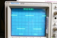
Measured today. 10 kHz square wave with STQ1NK60ZR-AP. (Why do they give them such awful names? That could be my password and meet all requirements)

Input (blue) is noisy and also has a bit of ringing that is faithfully reproduced by the preamp. Source is REW. For some reason, ARTA’s 5 kHz square wave was very poor. So much ringing that it is unusable. Still waiting on the cheapo function generator. But we can put to bed the thought of putting in a bypass cap on the PCB.
Input (blue) is noisy and also has a bit of ringing that is faithfully reproduced by the preamp. Source is REW. For some reason, ARTA’s 5 kHz square wave was very poor. So much ringing that it is unusable. Still waiting on the cheapo function generator. But we can put to bed the thought of putting in a bypass cap on the PCB.
When I worked in the advanced research department at Motorola we has to change our passwords weekly, were not allowed to write them down or have them stored in the computer. Each password had to be completely unique and not be based on any of your previous 10 PWs. They had to be 12 characters minimum. They instituted this policy in about 2009 after two major breaches, one of which was a human spy from an asian country working inside the Chicago plant. Of course there was a huge push back from many employees. This was discussed in a meeting where I explained that compliance was pretty easy requiring virtually no extra effort. I stated that my password was stored in plain sight on my desk, and challenged anyone to "crack my system." I, like many busy engineers did not have a spotlessly clean desk and a stack of data sheets was not uncommon. As you realized, part numbers often make good passwords, especially if you throw a random special character on the beginning or end.STQ1NK60ZR-AP. (Why do they give them such awful names? That could be my password and meet all requirements)
I eventually got all the parts I ordered from DK, and the box from Mouser came yesterday. It contains 4 X 650 volt UJ3N065080K3S SiC J-fets and several other parts. The J-fets are destined to be the source follower after a couple of UNSET gain stages. I need to put about 400 to 500 volts peak to peak into a 600 ohm output transformer. All will be tested with both tubes and solid state components. Unfortunately the parts shortage issue has made it impossible for anyone to build my two best selling PC boards, so most of the parts sitting on my desk are possible substitutes for CCS and LDO regulator chips. I will be testing this stuff first.Looking forward to it. Did you get your Digikey order?
Probably. I have found that saturation (running out of voltage headroom) is more common in this circuit than cutoff. Low voltage across the fet brings a different set of problems, but lower linearity is the biggest one.I am driving a VFET source follower with it right now and it needs 41 volts peak to peak. At 60 volts on the middle FET and 20 volts across the bottom one, there are 40 volts across the middle one, which means driving the VFET to full power will put the middle FET at a low of 20 volts (40-20), so we are far from cutoff. Am I doing this right?
Early versions of the "FetSet" that I saw on this forum had minimal voltage across the input fet because the gate was at ground potential. This can lead to some issues, especially if the driving source has a high output impedance. With such a low voltage across the fet it is operating in a region where all of it's capacitances are varying a lot with the applied signal. This can create a low pass pole that moves with signal frequency. Many of the tubes VS transistors debates of 10 to 20 years ago blamed this effect for Transient Intermodulation Distortion (a real phenomenon) and used it to justify the "all silicon is evil" discussions.
The FetSet curcuit here has some bias applied to the input fet to keep the voltage across it in a better place such that a two or more volt signal swing is not using up 100% of its range.
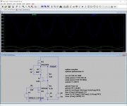
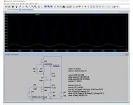
Enclosed are two LTspice simulations of a FetSet circuit. They are the same except for the input 1 KHz signal level. The green trace is the voltage on the gain fet and input fet's source. The blue trace is the gain fet's drain.
At 1 volt (peak) of input the input fet sees a two volt (peak to peak) variation in its source voltage (16.75 to 18.75 volts) This is about 10% of its available voltage. At two volts of input there is still plenty of headroom across the p-fet. The gain fet has 10.5 volts across it (27 - 16.5) ar the bottom of the sine wave. and 29.5 volts across it (48 - 18.5) at the peak of the sine wave.
Crank up the drive to 2 volts and we see that the gain fet starts to run out of voltage head room. This circuit has three active elements in series, so there is a balancing act to give each one its most possible headroom. LTspice simulations can get you in the ball park, but are only as good as the models used. Real parts often don't quite match the sim, so some resistor tweaking will be needed.
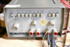
Back around 2000 Motorola used to sell surplus test equipment to employees. I picked up this HP3311A function generator for $20 and the Tek 2232 DSO for $100. The scope was on my desk at work for years but developed an intermittent condition thar required a good smack every day or two. It would occasionally do a spontaneous reboot whenever it was in the mood. During a random audit one day the inspector noticed that it and some of my other test equipment was say 5 to 10 years past its calibration due date. All the "non compliant" went to the cal lab where the scope was scrapped and replaced with a shiny new one since it was old, and the cal lab tech didn't know where to smack it. This model had known power supply issues. I bought the "dead" scope for $100, over 20 years ago and still smack it whenever it needs it, and it still reboots whenever it wants to. The scrap sale had a bunch of these function generators. I have no idea where in the plant they came from, but it works fine. I have never taken the covers off of either. Together they make pretty 10 KHz square waves.Without getting into controlled impedance interconnects and the like, that is about as good a square wave as you can expect to see from audio equipment.
Enjoy the preamp!
Attachments
Dear George,
I'm very glad you used my files to further develop the schematic.
I would like to share this other very simple yet effective circuit I've developed applying Rod Coleman's Shunt Cascode to SS devices.

I'm very glad you used my files to further develop the schematic.
I would like to share this other very simple yet effective circuit I've developed applying Rod Coleman's Shunt Cascode to SS devices.
Haha... that's a nice trick!As you realized, part numbers often make good passwords, especially if you throw a random special character on the beginning or end.
Nice! I got an SiC FET too in my last order. I actually plugged in that behemoth in this preamp circuit. Sounded decent.I eventually got all the parts I ordered from DK, and the box from Mouser came yesterday. It contains 4 X 650 volt UJ3N065080K3S SiC J-fets and several other parts. The J-fets are destined to be the source follower after a couple of UNSET gain stages. I need to put about 400 to 500 volts peak to peak into a 600 ohm output transformer. All will be tested with both tubes and solid state components. Unfortunately the parts shortage issue has made it impossible for anyone to build my two best selling PC boards, so most of the parts sitting on my desk are possible substitutes for CCS and LDO regulator chips. I will be testing this stuff first.
Yeah, it sounded okay with gate at zero volts, but definitely better with 20 volts or so betweeProbably. I have found that saturation (running out of voltage headroom) is more common in this circuit than cutoff. Low voltage across the fet brings a different set of problems, but lower linearity is the biggest one.
Early versions of the "FetSet" that I saw on this forum had minimal voltage across the input fet because the gate was at ground potential. This can lead to some issues, especially if the driving source has a high output impedance. With such a low voltage across the fet it is operating in a region where all of it's capacitances are varying a lot with the applied signal. This can create a low pass pole that moves with signal frequency. Many of the tubes VS transistors debates of 10 to 20 years ago blamed this effect for Transient Intermodulation Distortion (a real phenomenon) and used it to justify the "all silicon is evil" discussions.
Yeah, that makes sense (I think). The drain of the gain FET in my sim is at 65 V or so, and so there is plenty of headroom even at 2 V input. Node 005 is the drain of the gain FET.The FetSet curcuit here has some bias applied to the input fet to keep the voltage across it in a better place such that a two or more volt signal swing is not using up 100% of its range.
Enclosed are two LTspice simulations of a FetSet circuit. They are the same except for the input 1 KHz signal level. The green trace is the voltage on the gain fet and input fet's source. The blue trace is the gain fet's drain.
At 1 volt (peak) of input the input fet sees a two volt (peak to peak) variation in its source voltage (16.75 to 18.75 volts) This is about 10% of its available voltage. At two volts of input there is still plenty of headroom across the p-fet. The gain fet has 10.5 volts across it (27 - 16.5) ar the bottom of the sine wave. and 29.5 volts across it (48 - 18.5) at the peak of the sine wave.
Crank up the drive to 2 volts and we see that the gain fet starts to run out of voltage head room. This circuit has three active elements in series, so there is a balancing act to give each one its most possible headroom. LTspice simulations can get you in the ball park, but are only as good as the models used. Real parts often don't quite match the sim, so some resistor tweaking will be needed.
Here's the near final PCB, ready to go for a trial run. My plan is to get one or two made and iron out any mistakes or problems during mounting and operation. Honestly, I haven't done a PCB this complex before. Any help is appreciated. I'm not going to worry about the stoppers being a little further away just yet. Will test this PCB out and then see if we need to change anything.
I already noticed that the coupling caps need to have holes at different pitches. Will work on that. But please let me know anything you see. Thank you!

I already noticed that the coupling caps need to have holes at different pitches. Will work on that. But please let me know anything you see. Thank you!
Rahul,Here's the near final PCB, ready to go for a trial run. My plan is to get one or two made and iron out any mistakes or problems during mounting and operation. Honestly, I haven't done a PCB this complex before. Any help is appreciated. I'm not going to worry about the stoppers being a little further away just yet. Will test this PCB out and then see if we need to change anything.
I already noticed that the coupling caps need to have holes at different pitches. Will work on that. But please let me know anything you see. Thank you!
View attachment 1044768
Yes, please allow for large size film coupling caps.
Thank you.
Quick update. Making one more change to the PCB: turns out the AC bypass, C4 in the Spice schematic below and C102 on the PCB, has a huge influence on the sound. I discovered this while playing around on a test board. It was sounding edgy and so I kept trying other devices, but nothing was changing. So, I started looking elsewhere. Tried paralleling the electrolytic in that position with a Wima DC Link MKP cap and the difference was night and day. I had said earlier that this position did not influence the sound much and this was based on the fact that the sound was nice and liquid with a Nichicon electrolytic there. But clearly, it makes a difference.
I am making room on the PCB for a Wima DC link style MKP cap there.
Sending PCB out to manufacturing today.

I am making room on the PCB for a Wima DC link style MKP cap there.
Sending PCB out to manufacturing today.
Quick update: PCBs are on the way from China. There was some delay in shipping, but hopefully they will be here by the end of the week.
Recently tried the DN2535 depletion mode FETs and were very sweet sounding in the above configuration. Another good option to have.
Recently tried the DN2535 depletion mode FETs and were very sweet sounding in the above configuration. Another good option to have.
Looking forward to your updates!Quick update: PCBs are on the way from China. There was some delay in shipping, but hopefully they will be here by the end of the week.
Recently tried the DN2535 depletion mode FETs and were very sweet sounding in the above configuration. Another good option to have.
It’s here!!! Wow, it is big.
Suddenly I am very conscious about waste… hope this works, otherwise all that material and effort to get it here will be for nothing. It is also quite beautiful. Very happy with the shop. I tried to get it made in the US and Canada, but prices were ridiculous.

Suddenly I am very conscious about waste… hope this works, otherwise all that material and effort to get it here will be for nothing. It is also quite beautiful. Very happy with the shop. I tried to get it made in the US and Canada, but prices were ridiculous.

- Home
- Amplifiers
- Pass Labs
- Schade Common Gate (SCG) Preamp