
Thanks for catching! I had deleted that junction once already. Not sure why it appears again. KiCAD did crash once, so that might be it.
Yes, if you see anything else, would be very grateful for the feedback.
And thanks Zin, Vunce, and BRN. Will look at all the feedback tonight. Have to go to work now.
Yes, if you see anything else, would be very grateful for the feedback.
And thanks Zin, Vunce, and BRN. Will look at all the feedback tonight. Have to go to work now.
The horizontal wire crosses right at the point where the vertical wire meets the pin of the fet. The software thinks that you intended for all three wires to be connected to the pin. Move the horizontal wire further away from the fet and this won't happen. You should probably delete the horizontal wire and re draw it to break the connection that may be in the netlist.Thanks for catching! I had deleted that junction once already. Not sure why it appears again. KiCAD did crash once, so that might be it.
One rule I use to avoid confusion in wiring (either layout on pcb or point to point) is to not have any four way wire crosses connect. Many times you need allow non connecting wires to cross as that can still be necessary to keep the schematic organized. See the image for a couple of examples of changes I would make to keep the wiring clear.

Hi all , I have been following along unfortunately just a newbie so not much help but I'm excited to see the outcome , will you be offering any PCBs for sale?? - Thanks!
Hi there, yes, that is the plan. I am working on it right now. I plan to order a few boards and send them out for free to the folks on this thread. And then do a second run. Don't intend to make money off this--want to keep this as fun. Certainly couldn't have done it without the contribution of several folks, many of whom are on this thread. Just want to make it easy to build. The schematics are out there for anyone to try.
Last edited:
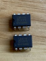
Tested the LBB110 bugger today. Works great! Tested with a meter and then with the amp. Upped the resistor feeding the input of the optocoupler to about 90k and the cap to 1000u, 16 V. Current feeding the LED is about 1 mA, and the 1000u cap charges slowly before the LED turns on and opens the switch (about 1 second I would hazard). Output doesn't go above a few mV. It doesn't work as well if you turn it off and then back on really quick, but I can live with that.
Neat little device this thing is.
Now, there is nothing left but to commit to the PCB layout. Hope to get done in the next week.
Neat little device this thing is.
Now, there is nothing left but to commit to the PCB layout. Hope to get done in the next week.
Last edited:
Good to hear the SSR works nicely, slick little bugger. Looks like one more hill to climb....Layout!

Layout is mostly done, part positions need to be finalized. But I am rethinking a few things based on feedback from all of you: cap sizes and test points. Also want to leave space for heat sinking and ease of use. On my test board right now, I am sticking different devices (TO-92 and TO-220) into a three-header screw terminal. I wonder if something like that would be convenient for everyone for popping different devices in... like tubes.
Here's the draft layout with the rats nest. Thoughts?
Nice! Cool little buggars!
Progress has been slow on the PCB--sorry--just been busy with life. Working on it right now though.
Progress has been slow on the PCB--sorry--just been busy with life. Working on it right now though.
Layout and routing done. Need to edit the text shown on the PCB and write helpful notes to make things easy to understand. Will post here for comments and feedback.
Meanwhile, here's a money shot courtesy of KiCAD:

Meanwhile, here's a money shot courtesy of KiCAD:
Yeah, it is a great software. I'm sure there are other, probably older software that folks here swear by. But for someone who is starting from scratch, such a fully capable and free software is a godsend. There is a learning curve and I'm sure there is lots to learn about PCB design, but it is easy to get started with some simple boards.
Been running some sims in LTSpice to check the bandwidth and explore an issue that George had raised about bypassing the Schade resistor to get better square waves. Adding any kind of bypass capacitance (even 10 pF) reduces bandwidth--at least in the sim.
For the STQ1NK60ZR-AP part, bandwidth is well past 1 MHz before hitting -3db (without any bypass cap across Schade resistor). For some of the other parts, dropping the Schade resistor to 10k (and other one to 1k) gives much higher bandwidth than with the 100k/10k pairing. The effect is that it bleeds some current, about 4-5 mA at 60V. I presume this charges the gate capacitance--I don't know. I'll listen to this change today and see if it sounds better. Even with the 100k/10k pairing, bandwidth is >100 kHz.
I didn't have a good 10 kHz square wave generator. Have ordered a cheapo board from eBay. Will see how well it can produce 10 kHz square waves and then test some iterations.
Meanwhile, working on finalizing the PCB.
I think bandwidth > 100 khz is more than adequate. Also, I strongly suspect if you build that layout with anywhere near the bandwidth you describe you will have massive oscillations. You don't have any stoppers on any active devices, and will likely need stoppers even if at much lower bandwidth. I wouldn't choose 1 mhz bandwidth over square wave or audio band performance. The purpose of the schade feedback is for triode like behavior and linearity at audio frequencies. It makes sense that the feedback will limit the bandwidth, but with that limit, the design would hopefully have better audio quality. As you lower the feedback resistor, you move farther away from the triode transfer curves you are trying to obtain with schade. There is likely a sweet spot though.
Thanks! Helps me understand this better.
The bottommost FET has a stopper. The top two form the CCS and have 220 ohm stoppers. The middle, gain, FET has no stopper. Does it need one?
So far, I have heard both the 100k and 10k versions and haven't noticed a difference. In fact, I slightly preferred the 100k version with the STQ1NK60 part. Also, the initial curve testing I did was with 10k/1k pairing. Got nice triode-like curves with that.
Is there a reliable way to check for oscillations? Will check square wave response after I get the generator.
- Home
- Amplifiers
- Pass Labs
- Schade Common Gate (SCG) Preamp