Green and blue leds are lit 🙂
But no sound. I'll check with my scope to see where the signal ends.
Regards
But no sound. I'll check with my scope to see where the signal ends.
Regards
But no sound. I'll check with my scope to see where the signal ends.
Regards
Ah but... do you have the 2 green LEDs on now (and the two blue chip LEDs in the clipping indicator section)? If you have the LEDs it would be good to also do another check of the power rails to make sure the voltages are still where they should be (no shorts).
Also remember about the input select switch on the front panel. Your input signal might be going to the other jack. If you are not using the attenuation resistors R31 and R32 you need to jumper them across with wire. R88 and R89 on either side of the 3.5mm output jack also need to be jumpered with wires. Those are place holders for damping factor resistors (that are not used in most of the builds).
Last edited:
Yes, two green and two blue shining. I will check voltages again tomorrow. I toggled the input select without luck.
Thank you agdr.
Regards
Thank you agdr.
Regards
Yes, two green and two blue shining
That is a good sign! JP17 below the input select switch is the output of that switch and the input of the gain stage. That's a good place to start with the scope. The metal shell of that input select switch is a good place to get the scope probe ground, or just one of the four ground pad holes.
Then JP12 and JP15 to the left of the blue LEDs are the output of the gain stage. Those feed the R31 & R32 attenuation resistors, then onto feed the pot.
One other thing comes to mind, the headphone relay. If that doesn't turn on you won't get any sound out. The delay should be somewhere around 3-4 seconds from when you power up to when that relay comes on. You can probably hear (or feel with a finger on it) the relay click if its working. I know you said that IC11 was running hot. Maybe there is a problem with that relay circuit. A good thing to check there is the voltage on the lead of C50 (cap in front of IC11 near the edge of the PC board) which is closest to IC11. That is the output of the IC11 relay circuit votlage regulator and should be somewhere around 24Vdc but with respect to the V- (JP19) point instead of ground. That is a tricky one - the relay circuit is rail to rail. The C50 lead you need to measure is under the PC board so you might want to solder a small test wire onto it temporarily. That is another change I made in V2.1, I added a test point right there for measuring the Vreg output. All the changes in V2.1 were minor cosmetic things like this and rotating JP19, nothing that affects the sound in any way.
Another thing to check is that your relay is labeled for 24Vdc and not 48Vdc. The 48v is for the +/-15Vdc build only and wouldn't even turn on at 24Vdc.
Last edited:
Right, I had missed the jumpers on R88/89 🙂. I have sound 🙂!
Thanks agdr!
Will listen to it further tonight and report.
Regards
Thanks agdr!
Will listen to it further tonight and report.
Regards
Turbon!!
Congratulations on "Sound"...this is good!!! LOL!
I hope you enjoy the ODA as much as I do!!
I recently built a tube amp that is highly touted as being great with high impedance headphones and its relly good, but the ODA is still in a class of its own!!
Enjoy..
Alex
Congratulations on "Sound"...this is good!!! LOL!
I hope you enjoy the ODA as much as I do!!
I recently built a tube amp that is highly touted as being great with high impedance headphones and its relly good, but the ODA is still in a class of its own!!
Enjoy..
Alex
Thanks Alex 🙂.
My sounds a bit raw. I expect it to grow more civilized after some hours.
But then again I'm still using not so good headphones which may explain it.
Regards
My sounds a bit raw. I expect it to grow more civilized after some hours.
But then again I'm still using not so good headphones which may explain it.
Regards
Turbon - congratulations on the successful build! 😀 That represents a lot of work.
Hey be sure to check the DC output offset level on each channel, if you haven't already. With the pots pre-centered with an ohm meter from the build instructions it should already be less than 200 microvolts or so. If you have a meter that can resolve down to 10uV or 1uV you can adjust the trimpots to get it even closer to zero. If your meter resolves to 1mV or 100uV it may just show zero, in which case best to just leave the trimpots as they sit.
Hey be sure to check the DC output offset level on each channel, if you haven't already. With the pots pre-centered with an ohm meter from the build instructions it should already be less than 200 microvolts or so. If you have a meter that can resolve down to 10uV or 1uV you can adjust the trimpots to get it even closer to zero. If your meter resolves to 1mV or 100uV it may just show zero, in which case best to just leave the trimpots as they sit.
Turbon - congratulations on the successful build! 😀 That represents a lot of work.
Hey be sure to check the DC output offset level on each channel, if you haven't already. With the pots pre-centered with an ohm meter from the build instructions it should already be less than 200 microvolts or so. If you have a meter that can resolve down to 10uV or 1uV you can adjust the trimpots to get it even closer to zero. If your meter resolves to 1mV or 100uV it may just show zero, in which case best to just leave the trimpots as they sit.
No, thank you agdr and everyone involved in the creation of the ODA. Sorry to say my oldish meters doesn't go further than 100uV - so zero have to do 🙂. Was there a new ODAC as well? Found it (small improvements - I'll use the original) 🙂...
I must say it has attitude 🙂. No need for the bass circuit.
Regards
Last edited:
What headphones are you using?
I have a set of Beyerdynamics T90's and DT 1350's and Audio Technical Mt 90's all which sound very well with the ODA.
I have several other amps and when I think one of them are better I go back to the ODA and am surprised at what I think might be better sounding isn't after listening to the ODA.
I think a lot of this is the expectation bias etc...
If your headphones are not that "great" that might be one of the reasons for the "raw" sound your experiencing etc...
Alex
Was there a new ODAC as well? Found it (small improvements - I'll use the original) 🙂...
George did make a rev B, but like you say the improvements are probably not going to be audible. The main thing was a fix for a problem where the ODAC just wounldn't work at all with certain PCs. Jon at JDS apparently tracked that down to an incredibly hard to find thing of certain rare PCs using ceramic capacitors on the power supply lines. Ceramics have a very low ESR. LDO voltage regulators are notoriously picky about ESR and that was just enough to cause the original vreg on the ODAC to go into oscillation. George has picked a new part that doesn't have the problem.
But long story short, if you are not having an ODAC problem with your PC (it either works or not and isn't subtle about it) no need to buy another ODAC.
And yeah, give the ODA a try with some better cans! 😀
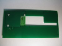
New ODA top-slot ODAC carrier board! And using pre-amp to re-buffer.
I finally got around to designing the top slot carrier board for the ODAC and matching back panel. 🙂
The board has a hole milled out of the center to allow heat from the output chips to make it to the top of the case and out a new row of vents in the (new) back panel.
The board layout, schematic (most complicated schematic you will run into here on the forum, lol!), and Gerber files for making your own boards are attached below. I've also added a new folder at the Google Drive link in the first post of this thread for "ODA top slot ODAC board", which has these same files in it.
The ODAC (either original or George's new rev B) is attached using three 3mm nylon bolts and nuts, as shown in the photos below. The ODAC board bolts down right on top of the carrier board. I've confirmed with George that is OK.
Note that the milled out section also solves one issue, as shown in the photo, that the 4 output wires go through the ODAC board and stick out the back. The carrier board would have required a hole there anyway. I just extended the milled-out section even though the ODAC board covers it.
The boards I've received today in the photos below are V1.0. I've just created a V1.1, which is what is in the layout and Gerbers below and at the Google drive link. The only change in V1.1 is that I extended the top of the milled-out section 2mm higher so it is flush with the top of the ODAC board, just for looks. 🙂 No functional difference.
I've included a ground plane on the bottom of the board under the ODAC area and included a solder hole to connect it to something. No need to connect it though, I just put that in for completeness. I've confirmed with George that having a metal plane 1.6mm under the ODAC like that won't affect anything on the ODAC.
The new rear panel has the hole for the ODAC USB port. I also left a round hole in case someone wants to solder on the ODAC's optional 3.5mm jack (requires jumpering the two sets of pads under the ODA). I wouldn't recommend using the ODAC's 3.5mm jack though - read the section below on rebuffering. It is a better way to go if you want your ODAC to also power RCA cables going to other equipment.
The new rear panels should be here in about a week. Once I verify the USB hole lines up properly with the ODAC USB connector I'll post that panel CAD out on the Google Drive link.
I've also had a chat with George about rebuffering, if someone wants to do that. NwAvGuy and George designed the ODAC to power the 10K load of the O2. Hooking other loads in parallel will increase the loading ont he ODAC an can potentially cause the ODAC distortion to increase, depending on the size of the load. George confirmed that the NJM455A, the surface mount version of the output chips in the O2 and ODA, would be a suitable chip for rebuffering if you want your ODAC to power long and/or higher capacitance RCA cables along with feeding an input on the ODA.
Well as luck would have it you can do that with the pre-amp buffer circuit and pre-amp outs on the ODA, if you are not already using them! 😀 So along with running your output wires from the ODAC to an input (rear RCA or front 3.5mm, holes by either) also run it to the input of the pre-amp chip (top and bottom pins of JP20). Then solder in a NJM4556A there and set the resistors to make it a unity gain buffer. The net result is the ODAC feeding one input of your ODA and also powering the pre-amp outs via the buffer chip. You will have no worries about how much capacitance your RCA cables have or their length with the output buffered like this.
Please note though that the pre-amp out does not go through a relay like the headphone amp out does, and the NJM4556A has that 3mV or so of DC output offset, so you might hear a small turn-on and turn-off thump in your speakers that you don't in your headphones. Another way to go is use a OPA2140 with 20 ohms of isolation resistance in series, using those pads (R57, R62) on the ODA board. Line level inputs at the other end of your RCA cables shouldn't care about 20 ohms. The OPA2140 has nearly zero DC output offset.
In the photos:
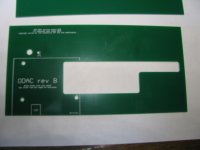
* 3452 and 3453 are the front and back of the board.
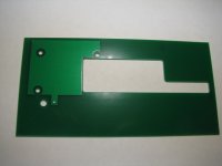
* 3454 is with the ODAC rev B bolted on with the nylon bolts
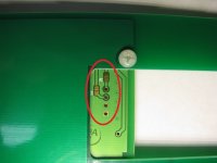
* 3455 shows the milled-out area where the output wires come through the ODAC board. Also the two jumper pads if you are using the ODAC's 3.5mm jack (again, not recommended).
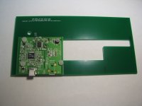
* 3456 shows the whole backside of the board with the ODAC bolted on.
The Gerber files to fabricate a board are in the attached .zip file. The README file has the parameters you will need.
I finally got around to designing the top slot carrier board for the ODAC and matching back panel. 🙂
The board has a hole milled out of the center to allow heat from the output chips to make it to the top of the case and out a new row of vents in the (new) back panel.
The board layout, schematic (most complicated schematic you will run into here on the forum, lol!), and Gerber files for making your own boards are attached below. I've also added a new folder at the Google Drive link in the first post of this thread for "ODA top slot ODAC board", which has these same files in it.
The ODAC (either original or George's new rev B) is attached using three 3mm nylon bolts and nuts, as shown in the photos below. The ODAC board bolts down right on top of the carrier board. I've confirmed with George that is OK.
Note that the milled out section also solves one issue, as shown in the photo, that the 4 output wires go through the ODAC board and stick out the back. The carrier board would have required a hole there anyway. I just extended the milled-out section even though the ODAC board covers it.
The boards I've received today in the photos below are V1.0. I've just created a V1.1, which is what is in the layout and Gerbers below and at the Google drive link. The only change in V1.1 is that I extended the top of the milled-out section 2mm higher so it is flush with the top of the ODAC board, just for looks. 🙂 No functional difference.
I've included a ground plane on the bottom of the board under the ODAC area and included a solder hole to connect it to something. No need to connect it though, I just put that in for completeness. I've confirmed with George that having a metal plane 1.6mm under the ODAC like that won't affect anything on the ODAC.
The new rear panel has the hole for the ODAC USB port. I also left a round hole in case someone wants to solder on the ODAC's optional 3.5mm jack (requires jumpering the two sets of pads under the ODA). I wouldn't recommend using the ODAC's 3.5mm jack though - read the section below on rebuffering. It is a better way to go if you want your ODAC to also power RCA cables going to other equipment.
The new rear panels should be here in about a week. Once I verify the USB hole lines up properly with the ODAC USB connector I'll post that panel CAD out on the Google Drive link.
I've also had a chat with George about rebuffering, if someone wants to do that. NwAvGuy and George designed the ODAC to power the 10K load of the O2. Hooking other loads in parallel will increase the loading ont he ODAC an can potentially cause the ODAC distortion to increase, depending on the size of the load. George confirmed that the NJM455A, the surface mount version of the output chips in the O2 and ODA, would be a suitable chip for rebuffering if you want your ODAC to power long and/or higher capacitance RCA cables along with feeding an input on the ODA.
Well as luck would have it you can do that with the pre-amp buffer circuit and pre-amp outs on the ODA, if you are not already using them! 😀 So along with running your output wires from the ODAC to an input (rear RCA or front 3.5mm, holes by either) also run it to the input of the pre-amp chip (top and bottom pins of JP20). Then solder in a NJM4556A there and set the resistors to make it a unity gain buffer. The net result is the ODAC feeding one input of your ODA and also powering the pre-amp outs via the buffer chip. You will have no worries about how much capacitance your RCA cables have or their length with the output buffered like this.
Please note though that the pre-amp out does not go through a relay like the headphone amp out does, and the NJM4556A has that 3mV or so of DC output offset, so you might hear a small turn-on and turn-off thump in your speakers that you don't in your headphones. Another way to go is use a OPA2140 with 20 ohms of isolation resistance in series, using those pads (R57, R62) on the ODA board. Line level inputs at the other end of your RCA cables shouldn't care about 20 ohms. The OPA2140 has nearly zero DC output offset.
In the photos:
* 3452 and 3453 are the front and back of the board.
* 3454 is with the ODAC rev B bolted on with the nylon bolts
* 3455 shows the milled-out area where the output wires come through the ODAC board. Also the two jumper pads if you are using the ODAC's 3.5mm jack (again, not recommended).
* 3456 shows the whole backside of the board with the ODAC bolted on.
The Gerber files to fabricate a board are in the attached .zip file. The README file has the parameters you will need.
Attachments
-
 IMG_3452.JPG88 KB · Views: 374
 -
 IMG_3453.JPG84.5 KB · Views: 367
 -
 IMG_3454.JPG107.8 KB · Views: 366
 -
 IMG_3455_1.jpg65.1 KB · Views: 366
 -
 IMG_3456.JPG74.8 KB · Views: 361
 -
 layout V1.1.png63.4 KB · Views: 129
 -
 schematic V1.1.png489 bytes · Views: 416
 -
Layout V1_1.pdf12.7 KB · Views: 113
-
ODA top sot ODAC carrier board V1.1.zip61.9 KB · Views: 119
-
README FOR GERBERS.txt433 bytes · Views: 77
Last edited:
Got my box and carrier board 🙂 Thanks agdr!
I'm sure I have read it somewhere but can't find it now. How do I ground the case? Same method as in the 02?
Regards
I'm sure I have read it somewhere but can't find it now. How do I ground the case? Same method as in the 02?
Regards
Got my box and carrier board 🙂 Thanks agdr!
I'm sure I have read it somewhere but can't find it now. How do I ground the case? Same method as in the 02?
Regards
Thanks for the update! The grounding happens automatically with the ODA. I have the lower right panel screw countersunk to cut through the anodization. When you put the nut on the 3.5mm input jack it grounds to the panel, then when you put on the panel screws it grounds the panel to the case.
Please be sure to read through the bottom part of post #820. The threads on the input jack won't stick out until the last little bit of the front and back panel screws are tightened down.
Last edited:
Boxed at last 🙂
Hi.
It's a very fine amp 🙂. Recomended! Tested now with my HD-650s and different ieds. Very strong and clear. I need to find the knobs with red lines as I only have blue and green ones available...
Thanks for all help and chering!
Regards
Hi.
It's a very fine amp 🙂. Recomended! Tested now with my HD-650s and different ieds. Very strong and clear. I need to find the knobs with red lines as I only have blue and green ones available...
Thanks for all help and chering!
An externally hosted image should be here but it was not working when we last tested it.
An externally hosted image should be here but it was not working when we last tested it.
Regards
Turbon!
Great looking ODA.....congrats and enjoy these indeed are "rare" head amps in the overall scheme of things!!
Alex
Great looking ODA.....congrats and enjoy these indeed are "rare" head amps in the overall scheme of things!!
Alex
Thanks Alex and CHiroshi. Yes, rare but hopefully the O2 community eventually will embrace the oda as it is better and stronger than the O2.
🙂 - I like IT airy... Going to Kjell tomorrow for an 18V/1A wallwart.
Regards
🙂 - I like IT airy... Going to Kjell tomorrow for an 18V/1A wallwart.
Regards
Last edited:
Turbon - congratulations on getting it all finished! 🙂 You are the first person I'm aware of who has used the silver case. Really came out looking nice.
PM sent about the knobs. 🙂
PM sent about the knobs. 🙂
Thanks for the offer on the knobs agdr. I'll look for other, bigger ones that I in the dark can feel it's the second one so it's the volume 🙂.
Running to clipping for 5 hours now - it has fewer - 39,2 centigrades... I will not put the ieds in my ears 😉. The box feels evenly warm - not hot at all. It will be cosy till the winter at night 🙂.
Regards
Running to clipping for 5 hours now - it has fewer - 39,2 centigrades... I will not put the ieds in my ears 😉. The box feels evenly warm - not hot at all. It will be cosy till the winter at night 🙂.
Regards
- Home
- Amplifiers
- Headphone Systems
- A version of an O2 Desktop Amp (ODA)