

And I'm measure speaker output and speaker gnd.
Reading around 1XmV to 1mV. Is it normal ??
That is normal ... as I said before R53/54 burn with no fuses ! Andrew T. suggested these and they have merit.
I do it different and just build up to the driver stage with 2 10R "sacrificial"
resistors on the rails before I go about "stuffin" outputs. Emitters of the drivers will be
+/- .6V with 2 68R's connected temporarily to the output coil.
NEVER a smoked output have I made (yoda speak
 ) .
) .To keep the Badgers "clean", consider "floating" R23
,27,32,33,36,37-41,50,53,54 slightly above the PCB or use "flameproof" devices.
OS

^
I make it a practice to lift all resistors off the boards by at leas 1/16 inch in all my amplifier builds, more clearance for high powered ones....
Best to keep "COOL". I also use 100R for R27 , this will set the VAS current source for 5+ mA (very cool).
This will not affect the compensation of the amp in any way. The Vbe resistor (R29-680R) will need to be changed to 560R to give
the same range for "Vbias" (R30).
OS
OS I just need clarification as I am checking all the updates. In post 1036 page 104 you have the 12V zener and C6 going to earth G2.
On the original circuit diagram they go to R16. Am I missing something?
Can't wait for the new PCB's!
Yes ! The new PCB will have the C-Z jumper as default (Z goes to G2-small signal ground).
With the R , you could reference it to EITHER the "virtual" ground of the LTP (.7V - AKA "luxman way") or to the same hard ground as "Z".
Options will still be available but a "build it this way or die"
is on the screenprint (below).
Will be PMing Variac with this "final".
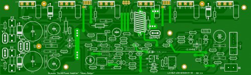
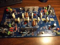
I just stuffed my boards (below 2), I know of NO lead space or hole issues.
Still need parts , not too economically secure.
More E-waste ! OS
Attachments

Ostripper,
That's a good looking layout! You've convinced me to order up a few boards.
That what I want to hear ... then this is the one that goes to Variac tonight.
I'll look over any fine points (45 degree angles + no sharp turns on corners).
Look over the screenprint for "ease of construction".
This layout has uniform .6mm+ spacing ,as well ...(UL 60950-1 Table 5B compliant
-DC voltages).
I thought hard on Q13 (Vbe device). For this circuit , the Cob of the devices
would "swamp out' any trace capacitance and having the Vbe cap (10-22uf)
real close to the jumpers virtually eliminates inductive issues (positive rail /output currents).
This style layout = EF2 only !!
A layout like this would not be ideal for a triple output. Any capacitance or inductive feedback
would degrade performance.
I must say
 , after assembling my Badgers, I was able to export the real world
experience to the upgrade in the layout. Still , the V2.3 board is more
professional looking and adheres to stricter design standards than just about
all the OEM amps I have ever repaired.
OS
Hi OS ,guys
I find the questions of my band.
The question is Q14,Q15.
I use TOSHIBA 2SC4793/2SA1837(F,M),it's bad in this band.
And I use onsmi MJE15032 / MJE15033 ,it's OK
2sc4793/2sa1837 are ok. That's what C18-c19 are for (high Ft driver).
Mje15032/33/34/35 are ideal and have higher current.
Both are OK.
OS
2sc4793/2sa1837 are ok. That's what C18-c19 are for (high Ft driver).
Mje15032/33/34/35 are ideal and have higher current.
Both are OK.
OS
OK!
OS
Thank you for your help
- Home
- Amplifiers
- Solid State
- diyAB Amp - The "Honey Badger"