Hi everyone,
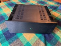
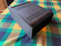
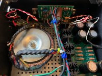
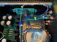
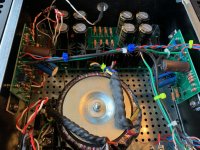
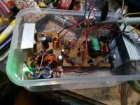
I'm finishing rebuilding a good old Sansui AU-111 from the early 70s, and now that's it has been thoroughly recapped, retubed and biased, i'm fine tuning it, hence I need some help.
Sorry for the long post but I wanted to provide as much information as possible, so the questions are a bit scattered through the post (the questions are in italic)
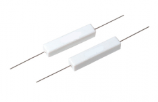
First thing I've done was to change the more than unbalanced volume pot by a 250K cms commuted one (with center tap), now both channels are exactly the same.
The old 250K pot measured 150K on both channels (IN to GND) and CT at 95k (from IN to CT)
Speaking of this, witch value should really be the center tap? 75K or 125K? (as it's a commuted pot I can choose my CT point).
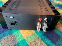
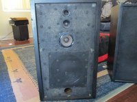
-I also shielded the power switch zone witch reduced induced hum significantly, still i'm getting audible hum with my efficient Heresy III at listening position.
When disconnecting Preamp stage from the main amp stage, I do not have any hum, perfectly quiet.
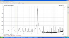
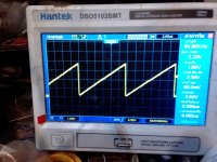
Where should I look at to hunt down this 50hz hum (frequency tested on scope)

-Last problem I have is related to the treble pot unbalance pointed by smurfer77 on AK forums. In fact my outputs are unbalanced and frequency response all other the place. All the tests I've done where made with an Analog discovery 2 using both Waveforms and Thatstuffmade audiosuite.
The balance pot was set at the middle position, treble and bass switch to "defeat".

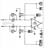
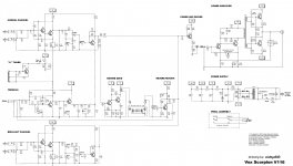
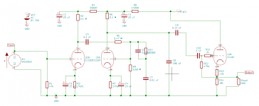
This is the preamp stage where trouble happens.
First thing I've done was to check if my balance pot was balanced by injecting signal directly at the volume pot input.


perfect balance on both channels, phase rotation is probably due to the fact that I'm using both generator outputs (I do not have this phase shift when inject mono signal on both channels)
When injecting from the treble pot center tap here's what I got:


clean
Then when injecting on the Tape monitor input (bypassing the phono stage)


Unbalanced output.
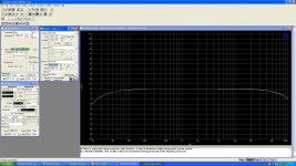
Now comes the frequency response curves:
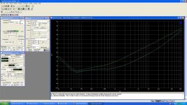
When injecting from Treble Center tap:

Volume pot at 90°

Volume pot at 180°

Volume pot at 270°
The channels are well balanced, the response is rolled of at the low frequency (I'm bypassing the feedback stage) and changes with volume.
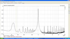
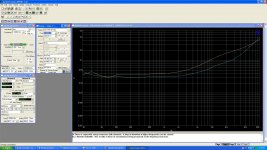
Now when injecting from the Tape monitor input:

Volume pot at 90°

Volume pot at 180°

Volume pot at 270°
Here the frequency response are full but varies with volume and the channels are not balanced anymore.
So my problem lies on the feedback circuit on V2/V3 second triode witch leads to the Treble pot witch sets the feedback loop resistance.
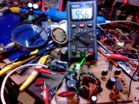
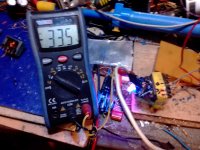
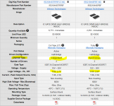
Here are the pot measurements on different points (I made the measurements with the pots in circuit)


 I have a significant difference in resistance between the two pots, the left one having more resistance, so I'm assuming I need to add resistance to the right one, but where should I put this resistance?
1. between the pot and the input (from v2/V3 first triode Cathode)

2. between pot Center tap and V2/V3 second triode Grid)

2. between pot and Feedback

I hope someone might help me on those issues.


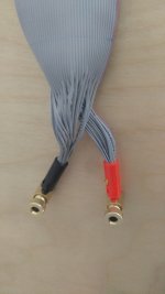
![IMG_3259[1].jpg](/community/data/attachments/771/771140-57a1562d387e688def0da9944073c496.jpg?hash=V6FWLTh-aI)
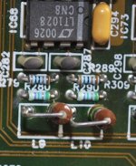
![IMG_3260[1].JPG](/community/data/attachments/771/771160-5ebe85022ad1bd8db26e82e131e5fc5c.jpg?hash=Xr6FAirRvY)
![IMG_3258[1].jpg](/community/data/attachments/771/771187-3537a326d7b2463e2290057fa356e63b.jpg?hash=NTejJteyRj)