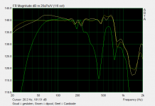
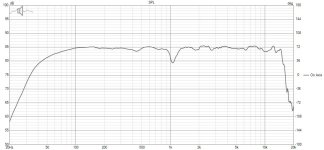
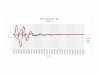
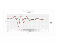
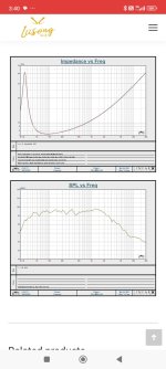
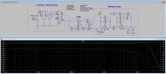
Comparison test DATS vs DATS+REW . Are the values at the left part of the chart OK? or caused by see INFO...
- By John64
- Equipment & Tools
- 9 Replies
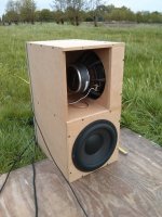
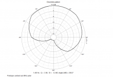
A 2.5 way basreflex loudspeaker floorstander with crossover was tested.
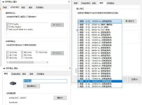
Multiple measurements are consistent and only differ at first impedance peak. 1 Ohm difference. ..Allways... what does this mean? Resister measurements outcomes between the 2 measure methods are the same.
Resister measurements that were done showed expected values and are within range for both methods.
Comparison measurement DATSv3 versus DATSv3 + REW
DATSv3 + REW Red
DATSv3 Purple

In REW all values except “the leads resitance value” for the impedance setup were take from the manual DATv3 on a Mac written by olen.
10kΩ for the Rsense value. (based on the value of output resistor) Don’t know my Dats R value
Set Rsense = 10kΩ
100kΩ for Rin (where is this value derived from?)
10mΩ for Rleads. I used 0.7399 Ohm Messured earlier with dats sofware.
For the reference cal I used a 4.952 ohm resistor..
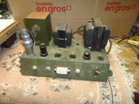
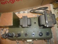
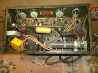
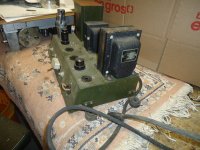
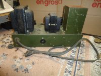
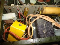
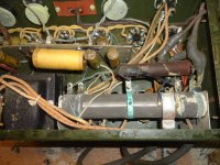
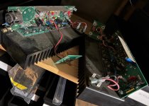
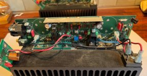
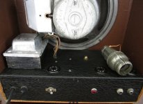
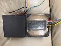
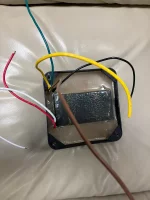
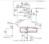
-- INFO -- My version of the DATSv3 is different from olen’s...See earlier post with picture...If my dats series output resistor value differs say 2000 Ohm from the 10000 in olens Manual could that alter the reponse, and then ONLY doing so in the left part of the graph we are seeing?
Thanks I appreciate your input and thoughts..
OS on laptop, Manjaro Linux with Wine installed....Linux version of REW 5.31.3 installed
install
DATS_V3_setup.exe installed with wine installer. (right click install with Wine windows program Loader)
Installation path: home/.wine/drive_c/Program Files/
Open console and type winecfg hit ENTER
In Wine configuration window that pops up click Add application. Go to c/Program Files/DATSV3/ and select en add DATS.exe
In Wine configuration window select the just added DATS.exe and click audio at top window
I chose windows version 7 but other OS may work.


For the input and output device now there’s the just installed PCM2900C Audio CODEC Analog stereo option to choose. The rest i left at “System default” cause other settings also didn’t add any specific in and outputs. In other words I CAN NOT CHOOSE “SPEAKER” OR “LINE IN” like olen could in the manual DATSv3 on a MAC.
Also in “PulseAudio Volume Control” I chose PCM2900C Audio CODEC profile: analog stereo Duplex

When in REW ...for input and output device same CODEC is chosen...in and output were left to default
No option to CHOOSE “SPEAKER” OR “LINE IN” I think I have might have to edit some settings in Manjaro or ad pipewire or jack to route audio ins and outs...If you guys think the measurement is ok I leave it as it is for now.
have a good weekend
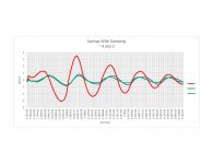
Multiple measurements are consistent and only differ at first impedance peak. 1 Ohm difference. ..Allways... what does this mean? Resister measurements outcomes between the 2 measure methods are the same.
Resister measurements that were done showed expected values and are within range for both methods.
Comparison measurement DATSv3 versus DATSv3 + REW
DATSv3 + REW Red
DATSv3 Purple
In REW all values except “the leads resitance value” for the impedance setup were take from the manual DATv3 on a Mac written by olen.
10kΩ for the Rsense value. (based on the value of output resistor) Don’t know my Dats R value
Set Rsense = 10kΩ
100kΩ for Rin (where is this value derived from?)
10mΩ for Rleads. I used 0.7399 Ohm Messured earlier with dats sofware.
For the reference cal I used a 4.952 ohm resistor..
-- INFO -- My version of the DATSv3 is different from olen’s...See earlier post with picture...If my dats series output resistor value differs say 2000 Ohm from the 10000 in olens Manual could that alter the reponse, and then ONLY doing so in the left part of the graph we are seeing?
Thanks I appreciate your input and thoughts..
OS on laptop, Manjaro Linux with Wine installed....Linux version of REW 5.31.3 installed
install
DATS_V3_setup.exe installed with wine installer. (right click install with Wine windows program Loader)
Installation path: home/.wine/drive_c/Program Files/
Open console and type winecfg hit ENTER
In Wine configuration window that pops up click Add application. Go to c/Program Files/DATSV3/ and select en add DATS.exe
In Wine configuration window select the just added DATS.exe and click audio at top window
I chose windows version 7 but other OS may work.
For the input and output device now there’s the just installed PCM2900C Audio CODEC Analog stereo option to choose. The rest i left at “System default” cause other settings also didn’t add any specific in and outputs. In other words I CAN NOT CHOOSE “SPEAKER” OR “LINE IN” like olen could in the manual DATSv3 on a MAC.
Also in “PulseAudio Volume Control” I chose PCM2900C Audio CODEC profile: analog stereo Duplex
When in REW ...for input and output device same CODEC is chosen...in and output were left to default
No option to CHOOSE “SPEAKER” OR “LINE IN” I think I have might have to edit some settings in Manjaro or ad pipewire or jack to route audio ins and outs...If you guys think the measurement is ok I leave it as it is for now.
have a good weekend


![IMG_4655[1].jpg](/community/data/attachments/1300/1300200-66e843a6707380c1edfc08398f5de42e.jpg?hash=f7ym8Jt2OM)
![[IMG]](https://i.ibb.co/fYQS9wK/P1020484.jpg "[IMG]")
![[IMG]](https://i.ibb.co/G08TSks/P1020489.jpg "[IMG]")
![[IMG]](https://i.ibb.co/tmfdxZg/P1000222.jpg "[IMG]")

![[IMG]](https://i.ibb.co/yhSdkzk/P1030220.jpg "[IMG]")
![[IMG]](https://i.ibb.co/pny1PHd/s-l1600.jpg "[IMG]")