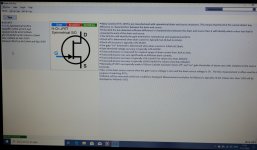
I used some time yesterday on 2SK209 (GR) measurement using a Peak DCR75 pro. I only have 10 2SK209 and I will use 8 so it was only to group them and also the see how close they are and also good to know they work. What is strange is that I don't agree with Peak DCR. What I think I have learned from this forum is that JFETs are depletion mode and Idss is the highest possible Ids at Vgs = 0V. So I think in the attached curve trace Idss = 4.2 mA and not 2.8 mA as indicated.
They write that if JFET is symmetrical it is not possible to detect D and S. But knowing that it is depletion mode and Ids declines when Vgs goes negative it should be possible to detect?
But anyway it is OK just the indicate the numerical Vgs value but I think the Vgs indication should be in "reversed order" in curve trace?
If not I am very confused")
Apart from that it is a pain to drop one of these devices on the floor. I used two hours searching the floor. I found it......but not on the floor. It was below the laptop…...but I think it would have been a pain to drop it on the floor
Next step is now soldering of the 8 SOT23 devices…….
They write that if JFET is symmetrical it is not possible to detect D and S. But knowing that it is depletion mode and Ids declines when Vgs goes negative it should be possible to detect?
But anyway it is OK just the indicate the numerical Vgs value but I think the Vgs indication should be in "reversed order" in curve trace?
If not I am very confused
Apart from that it is a pain to drop one of these devices on the floor. I used two hours searching the floor. I found it......but not on the floor. It was below the laptop…...but I think it would have been a pain to drop it on the floor
Next step is now soldering of the 8 SOT23 devices…….
Attachments
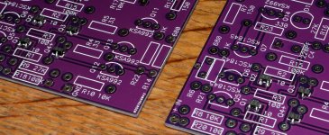
SMD solder of the 8 JFETs now finished and it went quite well taking into consideration that it was first time. These small things moves very easy so it requires a bit of patience and a steady hand. I invested in a Stannol Flux-Stift to clean the pads before soldering. With 0.37mm 63/37 solder and a 0.4mm Weller PCT no. 8 tip and cleaning afterwards with iso propanol it does not look too bad. There is a small "tip" on one of the solder joints which I don't like....but don't like either to heat it up again just for cosmetics……
Now the rest can be a bit more relaxed…...but need to order 15 ohm 1/2 watt resistors for the bigger output transistors.....and 5 pF capacitors for the feedback circuit.
Now the rest can be a bit more relaxed…...but need to order 15 ohm 1/2 watt resistors for the bigger output transistors.....and 5 pF capacitors for the feedback circuit.
Attachments
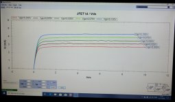
I found my error using the DCR Pro as curve tracer.
Now it looks as expected and shows "square law" between Vgs and Ids.
On data sheets they never show Ids when Vgs goes positive. Ids continues to increase when Vgs goes positive. Should probably keep it below 0.7 V.
Idss was about 2.9 mA on all devices which is in the low end for a GR.
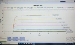
Now it looks as expected and shows "square law" between Vgs and Ids.
On data sheets they never show Ids when Vgs goes positive. Ids continues to increase when Vgs goes positive. Should probably keep it below 0.7 V.
Idss was about 2.9 mA on all devices which is in the low end for a GR.
Attachments
Best technique for soldering the smd’s..
Greetings! I am about to start stuffing the board and would like to know what is the most practical way to do that. I was condidering applyng a little bit of solder to all the contact surfaces, place the smd on the board trace and heat.... Is this ok? Thanks.
Greetings! I am about to start stuffing the board and would like to know what is the most practical way to do that. I was condidering applyng a little bit of solder to all the contact surfaces, place the smd on the board trace and heat.... Is this ok? Thanks.
Greetings! I am about to start stuffing the board and would like to know what is the most practical way to do that. I was condidering applyng a little bit of solder to all the contact surfaces, place the smd on the board trace and heat.... Is this ok? Thanks.
There are a number of YouTube videos and other sources demonstrating effective techniques. I'd recommend watching a few if you're new to SMD soldering. If you've never done it, I'd advocate getting a practice kit or finding something to practice on before soldering anything that "matters". I got a practice board for a few bucks, and it was well worth it.
More to the point and actually answering your question - If you are asking about hand soldering with wire vs. paste using a standard soldering iron - I would not recommend tinning all the pads prior to placing the parts.
I was a "first time smd solder" and there are some pictures just above of the result. I think it went quite well.
I invested in a very thin solder tip (0.4 mm) and thin solder wire (0.38 mm) with lead (63/37).
My technique was to first place the smd FET at the pads. Then with a steady hand heat one solder pad with solder tip without touching the component. Then apply a bit of solder also without touching the component. This cause that the component is fixed (but not soldered 100%). Then I just solder the two other pins and after that go back to the pin that was just fixed and make it 100%.
I also invested in a flux pen which I just used to clean the pads before placing the component at the pads (I don't think this is strictly necessary but it may be good practice). After soldering I cleaned using ISO propanol to remove solder flux.
<snip>...connect to a pair of MOFO boards (one attached to each heatsink, and biased to 2.5A each with a +24V DC supply) and then use it in a balanced input bridged output configuration. Output impedance will double (damping factor will be 20), so about 0.4 ohms output impedance. Should get you loads of power in class A (~nearly 100 watts) ... </snip>
Shouldn't that be 50watts, for bridged MoFos (24V 2.5A), and then only if you're loaded with 16 ohms? Bridging them doubles the drive voltage, but doesn't increase the available current because of the choke loading - you can't sink more than the Ibias, 2.5A here. The high side amp can source more than 2.5A by turning on the MOSFET harder; the low side amp can only turn the MOSFET all the way OFF, so can't sink more than the 2.5A choke bias current.
Now, in Parallel mode, you get twice the current, but same drive voltage. TANSTAAFL.
(There Ain't No Such Thing As A Free Lunch)
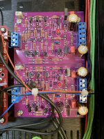
It was actually a week ago but I'm finally getting around to posting the photos... Here's the stereo PCB installed and working beautifully. 
The were a few silkscreen changes done, but nothing to the layout, they work perfectly. They will be sent for production and be in the store in however much time that takes.
The were a few silkscreen changes done, but nothing to the layout, they work perfectly. They will be sent for production and be in the store in however much time that takes.
Attachments
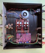
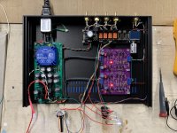
Here’s an in process, powered up, pic sans face plate (making my own), in a 1U store chassis.
Learned(ing) a ton of course... can’t wait to give it a listen!
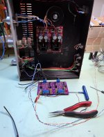
Setting offset was very predictable, no floating around, zeroed easily. Especially after fixing a bad SMD connection on one side (thanks 6L6!).
@6L6: will this qualify me for Iron Pre adventure? more more more! haha.
Learned(ing) a ton of course... can’t wait to give it a listen!
Setting offset was very predictable, no floating around, zeroed easily. Especially after fixing a bad SMD connection on one side (thanks 6L6!).
@6L6: will this qualify me for Iron Pre adventure?
more more more! haha.Attachments
6l6,
Is the output offset trim pot as sensitive as the first version?
The offset pot was sensitive? Are you sure you’re not thinking about the BA-3 as preamp?
The offset trim pot responds easily and well, there’s no mystery or crazy sensitivity.
@pfarrell
Nice build! Can you give a link to the psu board your using?
I have the same screwdriver, super handy multi-bit tool
Thanks!
LR Phono Preamp (Millett designed it for his phono pre (which looks interesting in and of itself), 6L6 brought it to my attention.)
He sells on ebay:
DIY PCB - Bipolar (opamp) power supply | eBay
I’m getting just under 20vdc +/- from it—could easily tweak it lower or higher. It’s nicely compact. I speced shorter sinks than what’s in the BOM, to fit 1U height.
Thanks 6L6. I agree it responds easily and well but takes a very small amount of pot turning to move the output voltage a lot. It’s all good, maybe I am being too picky. Can’t wait for the store stereo version, they will go fast because it is an excellent line stage and I am sure that everyone that has built one would highly recommend it. Thanks Wayne.
- Home
- Amplifiers
- Pass Labs
- Wayne's BA 2018 linestage