The AVCC circuit I used is the one attached to post $3003. No other components or connections.
Using copper foil for a makeshift ground plane is not a new idea. It kinda works, but the foil is pretty thin.
Did you choose that over a piece of double clad PCB because the op-amp DIP doesn't have any pins directly soldered to ground? Or another reason?
I was thinking of double clad since it could be tacked/soldered to the bottom ground plane in a few places along one edge. Maybe single clad would be better.
Any idea why the output filter caps are so large (6.8nF, C25 & C26) and the series resistor so low (200 Ohms, R17 & R18) in post 3003?
Just wondering why it is such a large value instead of something like 1nF.
Together with R17/R18 it's yet another pole (R7/C15 and R8/C16 is the first) at about 100KHz, part of the output LPF.
BTW, here's the schematic for your chinese junk board.
My advice, dump this abomination and get something decent. This board is unfix-able to anything measuring decent. Besides, you won't be able to hear any improvements you may bring, anyway.
EFCノート: ES9038Q2M DAC内蔵ヘッドホンアンプの製作 (1) DAC基板の改造
My advice, dump this abomination and get something decent. This board is unfix-able to anything measuring decent. Besides, you won't be able to hear any improvements you may bring, anyway.
EFCノート: ES9038Q2M DAC内蔵ヘッドホンアンプの製作 (1) DAC基板の改造
Last edited:
Together with R17/R18 it's yet another pole (R7/C15 and R8/C16 is the first) at about 100KHz, part of the output LPF.
Thank you for the schematic for the board.
I do realize it is part of the LPF. I was just wondering why such a large cap and small resistor. (As opposed to a smaller cap and larger resistor that still had the same RC product.)
I think that is the first time I have seen more than 1nF on the output of a DAC filter (or preamp or the input of a power amp).
From a frequency response perspective, it is the RC product that matters. C=1nF would require R=1.5k; I don’t see why increasing the output stage output impedance in the pass band would be a good thing, it would only make it more sensitive to the next stage input impedance. 220ohm is acceptable as a compromise.
My original stance is unchanged; as no doubt is yours")
Actually I have found some of the discussion interesting. If I ever get serious with building an ESS dac I certainly will look more into discrete regulators for AVCC. However I would still rely on measurements since I'm not a believer of "design-by-sound" alone. And I still would not use boutique components but decent bog-standard stuff that meets the requirements
BTW, here's the schematic for your chinese junk board.
My advice, dump this abomination and get something decent. This board is unfix-able to anything measuring decent. Besides, you won't be able to hear any improvements you may bring, anyway.
EFCノート: ES9038Q2M DAC内蔵ヘッドホンアンプの製作 (1) DAC基板の改造
Yes, the board is actually so bad that the blogger cut his board in half (pictures 3 and 4)

Actually I have found some of the discussion interesting. If I ever get serious with building an ESS dac I certainly will look more into discrete regulators for AVCC. However I would still rely on measurements since I'm not a believer of "design-by-sound" alone. And I still would not use boutique components but decent bog-standard stuff that meets the requirements
Me too mate. All good, I was just conscious of derailing the thread too much; although it was conversation that would hopefully be of interest to the thread. I'm totally with you on the measurements. Controlled listening tests should not be disregarded either, but not as a means to make sure you are able to meet the objective capabilities of the parts used; at -140dB. AVCC is certainly an area that needs proper attention paid; given the lack of PSRR and as I mentioned, for me, its also as much about the challenge of the design aspects; objectively and aesthetically.
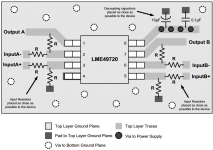
One free upgrade for SMD bypass caps. USE 2 or 3 vias per terminal in your patterns instead of 1, to lower the inductance. this is when placing directly under the DAC. on top, make a ground island and use a whole bunch of vias, but I prefer underneath, to free up routing.
If anything i'm guilty of over-speccing parts; objectively. I'm also guilty of a bit of bling, but usually recognise it as such and never at the cost of worse performance. Also, many people take my tone as harsh, but it's not often intended as such.
Last edited:
Wow, looking at the schematic; that is certainly a proper piece of crap ... ha!!! indeed, definitely not in current mode. i'm not sure the designer is aware of the difference and probably just copy-pasted an opa voltage buffer application from one of their (or someone else's) other boards; then cut as many corners as possible.
One free upgrade for SMD bypass caps. USE 2 or 3 vias per terminal in your patterns instead of 1, to lower the inductance. this is when placing directly under the DAC. on top, make a ground island and use a whole bunch of vias, but I prefer underneath, to free up routing.
Maybe like the attached tutorial.
Attachments
Yes, the board is actually so bad that the blogger cut his board in half (pictures 3 and 4)
Wow, looking at the schematic; that is certainly a proper piece of crap ... ha!!! indeed, definitely not in current mode. i'm not sure the designer is aware of the difference and probably just copy-pasted an opa voltage buffer application from one of their (or someone else's) other boards; then cut as many corners as possible.
all this was crystal clear back in 2017 when this thread started. I understand, that it is boring to dig through all those thousands of posts, but still... for me the board was just a module to experiment with, since in those glorious days no DS were available for ESS DACs. from this "piece of crap" I learned what matters here and built a PRO chip DAC, which I still enjoy.
so what then is your point guys?
Last edited:
Not Boring; not going to happen. I was never a potential customer for this board. I myself am not asking for help, so you can read, or not and i'm certainly not required to read the whole thread to comment.
As for my point. Modding is certainly a way to get your feet wet and sometimes there are boards that are well placed to be upgraded with a few mods, but when a design is so broken, like this one, you are much better served to just spend a bit more on the dac to begin with. With the ESS parts and datasheets now available to anyone that wants to buy them at Mouser, there will be a lot more projects available here at DIYA.
Hopefully someone doesnt have to read the whole thread now to find that out.
if you want to do it right, DAC chip and I/V should be on the same board. if not, then a simple protoboard will allow you get rid of some 20dB of distortion, as indicated in ES9038Q2M Board
btw, highly prised PRO-JECT PRE BOX S2 DIGITAL measures about the same (at least the piece I have), sounds a bit better though.
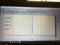
yes, and for those measuring thirsty here I attach the graph for ES9028pro with a discrete AVCC PS onboard, and LT3045 for digital and LT3042 for the clock.
certainly for the correct measurement one would need to use a rejector, but I was too busy enjoying the music that I never did this
btw, highly prised PRO-JECT PRE BOX S2 DIGITAL measures about the same (at least the piece I have), sounds a bit better though.
yes, and for those measuring thirsty here I attach the graph for ES9028pro with a discrete AVCC PS onboard, and LT3045 for digital and LT3042 for the clock.
certainly for the correct measurement one would need to use a rejector, but I was too busy enjoying the music that I never did this
Attachments
Last edited:
Any idea why the output filter caps are so large (6.8nF, C25 & C26) and the series resistor so low (200 Ohms, R17 & R18) in post 3003?
Yes. As Syn08 pointed out, its the time constants that matter and the 220-ohm resistor is an engineering compromise. We need to be able to drive a reasonable range of input impedances that may be found in downstream audio equipment. Also, some may remember the previous explanation about using a gaussian filter type to help preserve waveshape as viewed in the time domain, particularly at lower frequencies where the ear may be sensitive to it. The difference between a gaussian filter and other commonly used audio filters such as bessel or butterworth is the location of the poles, the time-constants. The 6.8nf cap is chosen to give one of the needed time constants.
It may help to think about an output stage like that in post #3003 as a circuit that is designed to be as simple as possible while at the same time satisfying a number of design other goals. We need it to do I/V conversion, filtering of RF and ultrasonic noise from the dac, removal of DC offset, differential summing of dac outputs, have low distortion, have low noise, and whatever else. How can we do all that with only 3 opamps? Of course, we could have used a bigger resistor and a smaller cap for that last time constant, but might then need to add a buffer stage after that to drive low-ish input impedance amplifiers. We could do that, but there is no free lunch, there will be some cost to it somehow or other.
Regarding the topic of modding a dac like this one or buying a reasonably good one (which is now an option, wasn't always that way): Maybe worthwhile to consider what is in a $250 dac, or even $6,000 dac. A rough estimate we can use is that the incremental, per-unit sold, markup on most consumer products is in the range of 3 to 5 times the manufacturing cost. That includes the case, the shipping box, the manual, everything. For high end audio, because the sales volumes are so low the markup has to be more like 6 times manufacturing cost. Other costs are covered by the markup factor: development costs, advertising, distributor markup, retail markup, etc.
For a high volume dac like D50 which retails for around $250, say we divide that by an average markup factor of 4 times. That means the cost of if making one must be limited to around $60.
On the other hand, for a $6,000 dac the manufacturer can spend around $1,000 to make one.
Okay. If we then ask what would adding two Crystek clocks at $25/each add to the the retail cost of a commercial dac? Anyone can do the math. Now add a dedicated high performance voltage regulator for the clocks, plus if its a really exotic design maybe good quality film bypass caps for the clocks instead of X7R high-k ceramic.
I think we can all see where this is leading. A lot of people around here really want the equivalent of a $6,000 or $15,000 dac, maybe more expensive. But they don't want to pay that much. And they don't care about the fancy case needed to sell dacs in the high end market. The problem is folks don't know how to do all the engineering to optimize good use of all the parts they are buying in order to diy it. They end up hacking expensive parts together in poorly engineered way and eventually decide what they have is good enough. IMHO included in that situation are some of the popular GB building-block subsystems diy'ers may believe will make for a great diy dac.
What a mess. All I can do is try to help as I can. I can talk about things that are public domain already. I can't give away proprietary information I am privy to. When it comes to that stuff I can give sort of veiled hints on where to experiment, but that's as far as I can go.
Last edited:
- Home
- Source & Line
- Digital Line Level
- ES9038Q2M Board