Eziitis,
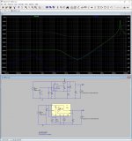
It would be very nice if Pavel would retry that simulation of the LT3042, with 10uF output capacitance, instead of the simulated 470uF. It is not by accident that the producer strongly recommends that filter capacity value.
With 10uF we will get back the claimed min. 1Mhz bandwith, which dictates the response inside 1usec instead of the <<16usec claimed in the sim..
Could we say that maybe it had been set up on purpose..? No that cannot be. On a positive note I see that a minimum bias current of 60mA had been maintained, at least.
Otherwise the result, cca 10mohm output impedance is not that far from reality. I have measured cca 5mohm, or a bit better, with 1MHz bandwith. Rising to 20mohm at 2Mhz.
Question is, and I had already suggested it to You: an LT3042, VSON package, can be organized in cca 10mm*10mm area. Or less.. And so, some mm away from the Dac VREF pins.
How many mohm are say, 5cm pcb trace (not plane)..?
What does it worth, a theoretical uohm regulator, dozens of mm away from the load?
Ciao, George
Maybe Pavel should also simulate PSRR (green is discrete, blue LT3042).
But anyhow simulations at these low levels are not to be taken as references. Implementation details (such as trace lengths as George mentioned) may totally turn the table.
So, please only measurements as evidence. Ok, results from controlled listening tests are also fine as evidence 😀
Attachments
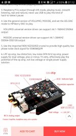
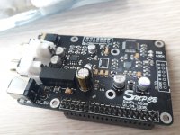
Anyone using this i2s DAC HAT for pi? Any recommend mod is highly appreciated. (It seems less room for modding).
ES9038q2m OPA1612 Op Decoder Digital broadcast board I2S 32bit/384K DSD128 for Raspberry pi 2B 3B 3B+ DAC G3-001
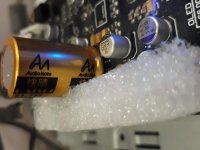
I just upgraded 1 cap (Audio Note) with wima 0.1uf in parallel.
ES9038q2m OPA1612 Op Decoder Digital broadcast board I2S 32bit/384K DSD128 for Raspberry pi 2B 3B 3B+ DAC G3-001
I just upgraded 1 cap (Audio Note) with wima 0.1uf in parallel.
Attachments

Yeah, my argument in favor of 'Discrete' regulators, such as the type Syn08 knows all too well from his long running phono/pre amp experiments, well documented on his site (thankyou very much for that btw mate!) is more just having fun with the design.
The LT3042/5 is not a cheap IC to implement properly, so, if designing your own board, its not hard to put together a buffered reference (shunt or series) for roughly the same—or at least similar—BOM cost. to get the most out of the 3042, the reference needs to be bypassed/filtered quite well; to the point of dominating the space taken up by the regulator. then add the optional external transistor that is optionally specified in the DS for higher current and you may as well build discrete IMO.
Now, im not making any claims for much higher performance, the 3042 is a really great chip and hard to beat, but I think the claim of 10 x 10mm is a bit optimistic. Using modern layout technique and SMD parts (LFPAK56 or smaller, for the mosfet), the added PCB area required by 'discrete' will be negligible (to the point of not making much difference to how close you could get it to the chip) the 3042 also has fairly ordinary PSRR at HF, so wants pretty decent filtering before it.
As for slapping 560uf across everything on the board, the 3042 dynamic performance is negatively affected by having too much capacitance on the load; as are many high performance regulators.
Last edited:
As for slapping 560uf across everything on the board, the 3042 dynamic performance is negatively affected by having too much capacitance on the load; as are many high performance regulators.
These boards don't come with 3042 or any high performance regulators for that matter. They have only LM7805 and AMS1117-3.3 on them.
By dynamic performance I assume you are referring to either line or load regulation? If so, would the combination of AMS1117-3.3 + 560uF ultra low ESR be better or worse (and in what way) on these boards?
The LT3042/5 is not a cheap IC to implement properly, so, if designing your own board, its not hard to put together a buffered reference (shunt or series) for roughly the same—or at least similar—BOM cost. to get the most out of the 3042, the reference needs to be bypassed/filtered quite well; to the point of dominating the space taken up by the regulator. then add the optional external transistor that is optionally specified in the DS for higher current and you may as well build discrete IMO.
Now, im not making any claims for much higher performance, the 3042 is a really great chip and hard to beat, but I think the claim of 10 x 10mm is a bit optimistic. Using modern layout technique and SMD parts (LFPAK56 or smaller, for the mosfet), the added PCB area required by 'discrete' will be negligible (to the point of not making much difference to how close you could get it to the chip) the 3042 also has fairly ordinary PSRR at HF, so wants pretty decent filtering before it.
As for slapping 560uf across everything on the board, the 3042 dynamic performance is negatively affected by having too much capacitance on the load; as are many high performance regulators.
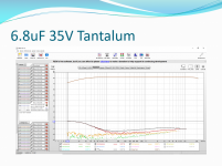
Much of what you wrote is not exactly based on facts. I have used LT30xx in several designs. The BOM costs for basic LT3042 regulator (as shown in the previous simulations) is about 6 euros. There is no need for anything special on the reference. X7R 1206 4u7 works fine as bypass to Rset. The whole regulator fits to about 8x12mm. As for the external transistor we are discussing powering AVCC on ESS dacs. I hope nobody is suggesting to use a single regulator for the whole ESS chip. And with regards to PSRR at HF LT30xx is fairly extraordinary (79dB at 1MHz or even to 10MHz).
The simulation shows 10mA load variation from 60 to 70 mA at 50 kHz. Where exactly on the datasheet do you see that on AVCC?
But there is an easy way for you to support your statement. Please provide one measurement of an ESS dac with your discrete regulator. You can pick any standard measurement to your liking. Then it should be relatively easy to compare that measurement to ASR's measurements of a DAC with the same ESS chip but without discrete regulator. If what you state holds water there should be something visible of the claimed better performance of discrete regulator.
Dear bohrok2610, please, just relax and ignore all this if you think it is a BS. I shared what worked for me and I do not care whether anyone accepts this approach or dismiss it. You say I am wrong. Fine, you could be proud you protected innocent and unexperienced readers to get mislead and loose time and money. So, please do not bother to tell me what kind of evidence I need to provide. Period.
Kozard...
Did you measured noise on power supply with a scope to see what happened with adding so big caps. Put 1khz into digital input and measure what happenes.
My approach is bring as clean voltage as possible on the board and there some small and high quality caps. Pps, pml in small size because no space for big foil caps. Sunting noisy lines with big caps just supress noise into gnd. Pcb gnd is poor so noise is flowing all over the board and mix with other noises.Problem is that noise pass back to circuit trought caps and resistors... if board would be 5layer it will be much easier to filter noise. But noise and thd numbers are not all that matters. Choosing the right material brings own sound charracter of the Dac.Bypassing power sopply lines with ceramics or pps , pml gives different sound charracter.
I guess I wonder how the geometry and the location of the noise generation relative to the bypass capacitor affects the current flow in the ground layer. It is just a hobby for me but it would be fun to have a simulation from Momemtum, Sonnet or Q3D. I don't think that will happen but a nicely colored graphic showing current distributions would be great to aid understanding. Maybe someone else has such a graphic that they could display from working on a similar problem?
Can you limit the flow of current by placing a broadband short very close (geometrically) to the source of the noise? For example, if you are dealing with noise generated by a microprocessor on the board would a broadband short placed very close to the microprocessor supply pins help contain the currents to mainly within the local geometry of the layout and ground plane? (Local to that microprocessor and the ground plane that generally encloses the micro and the associated capacitors and ground vias used to form the broadband short?)
I did build a 60 dB LNA so that I can examine actual data regarding noise. (Picture attached.) I was planning to use that later once I bought the low noise regulators and also started to make the op-amp based (filter type) AVCC supplies.
As for capacitor types I am generally only concerned about non-bypass usages such coupling capacitor or filters in ultra-low distortion circuits. Thus I read about measurements on capacitors and performed some of my own (signal coupling) distortion measurements. (Two illustrative examples are attached.) When bypassing my general approach is to keep the voltage across the capacitor constant. I try to make a nice broadband short using an appropriate combination of small to large capacitors. Obviously on this board I can't change the layout but if I was making a layout I would place the capacitors and ground vias as close as possible. For bypassing what is your concern regarding capacitor type?
I recently assembled an ultra-low distortion headphone amplifier with 8x parallel high current op-amps with the intent of extending the range of my distortion measurements. However my concern was not for bypassing. Are you perhaps concerned about insufficient bypassing (when the capacitors are too small) where there are large ripple and noise voltages remaining riding on top of what you want to be DC instead? (And then perhaps being distorted and generating harmonics of the ripple and noise?)
Attachments

Last edited:
Have you measured the noise on the various power supplies on the board prior and after adding those Oscons? Just measuring on the output does not reveal which of these fixes have been beneficial and which not. Hanging capacitors and wires may easily pickup rf noise.
InspectorGadget,
Very reasonable thinking, thanks.
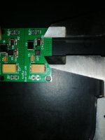
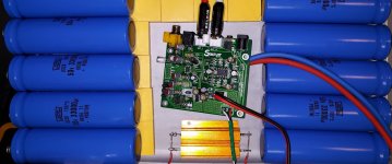
What regards the space, yes I was exagerating a bit - though not too much? See photo, there I was really not 'sparing' sul quality, 1206 precision set resistor, 1210 filter cap (PPS), PMLCAP in output. 1cm is indicated.
On a board, the big input capacitor is not really needed.
(while with a floating board the inductance of the external wiring harness should be absorbed by some more uF)
Very reasonable thinking, thanks.
What regards the space, yes I was exagerating a bit - though not too much? See photo, there I was really not 'sparing' sul quality, 1206 precision set resistor, 1210 filter cap (PPS), PMLCAP in output. 1cm is indicated.
On a board, the big input capacitor is not really needed.
(while with a floating board the inductance of the external wiring harness should be absorbed by some more uF)
Attachments
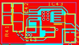
Here is a 2-layer LT3042 layout that I have used on some designs. This uses the "easier-to-solder" MSOP package. Caps are 1206 and Rset is 0805. The whole regulator fits within 14x8mm (blue rectangle). Note also the "Kelvin-connected" output capacitor as recommended by the datasheet. Don't know if it is actually doing any good 😀
Anyhow one of the advantages of the small space required is that once you have a decent layout it is easy just to copy-and-paste the same layout on other designs.
Anyhow one of the advantages of the small space required is that once you have a decent layout it is easy just to copy-and-paste the same layout on other designs.
Attachments
Nice!
And yes, the Vson package is PITA..
And me too, have implemented the recommended Kelvin connection. Four layer board, but only because the 'dual' structure, with the LT3094. And more heatsinking capability.
And yes, the Vson package is PITA..
And me too, have implemented the recommended Kelvin connection. Four layer board, but only because the 'dual' structure, with the LT3094. And more heatsinking capability.
kozard,
Most of the distortion problems you see get much, much better with a properly laid out output stage and with a proper AVCC supply. There are also other factors that will effect the sound that may not show up on an FFT very well, if at all. A spectrum analyzer can be handy. Also good to have a fast scope with dot averaging (rather than just sweep averaging). A Timpod would be great too. Since instruments that can be used to find some types of problems and verify fixes can be expen$ive, IME its also possible to use good engineering practices, thoughtful experimentation, and dare i say, skilled listening. The latter is a complex subject I won't go into for now.
Most of the distortion problems you see get much, much better with a properly laid out output stage and with a proper AVCC supply. There are also other factors that will effect the sound that may not show up on an FFT very well, if at all. A spectrum analyzer can be handy. Also good to have a fast scope with dot averaging (rather than just sweep averaging). A Timpod would be great too. Since instruments that can be used to find some types of problems and verify fixes can be expen$ive, IME its also possible to use good engineering practices, thoughtful experimentation, and dare i say, skilled listening. The latter is a complex subject I won't go into for now.
Much of what you wrote is not exactly based on facts. I have used LT30xx in several designs. The BOM costs for basic LT3042 regulator (as shown in the previous simulations) is about 6 euros. There is no need for anything special on the reference. X7R 1206 4u7 works fine as bypass to Rset. The whole regulator fits to about 8x12mm. As for the external transistor we are discussing powering AVCC on ESS dacs. I hope nobody is suggesting to use a single regulator for the whole ESS chip. And with regards to PSRR at HF LT30xx is fairly extraordinary (79dB at 1MHz or even to 10MHz).
Oh, I see, you are the arbiter of fact around here eh?
lol, the BOM is 6EU? the chip alone is more than 5EU at digikey in single quantities. you are correct re PSRR at 1MHz, it was the drop needing to be kept within a very specific and low range to keep the DS performance; thus preferring a regulated input to keep Vdrop lowish and tight. it doesnt like heat
its a great chip, but to match the datasheet headline noise performance and Z-out to actual measured application; it needs rather specific load capacitance, voltage drop and layout. that is a fact; like it or not, that is the reality uncovered by Jan Didden, Gerhard and co, who have been using it to its limits and posting measured (not simulated) results for years.
i've been designing for 9038PRO, so 100-110ma is needed for each VREF, so while the 3042 or 3045 will of course do it, I can throw maybe $2 more (if that) at an LED string/zener->opa1611/lt1028/AD825/LME49990+filter->P-FET and have more fun doing so, while using a meaningless amount of extra board space. I have strips of just about everything needed already in my parts bin and the board space and design between the 2 is no meaningful difference in application at all; we arent trying to fit the whole dac in a matchbox. I can fit it (the 'discrete' reg) in 20x15mm (much smaller for lower currents) More time in the design for 'discrete' but not all that much and who cares?
i'm not even discouraging the use of chips. I like them. I even like the 3042/5 and may end up using it for Vref if I cant get close, or better its noise and Z-out. I have a layout for it already. Its fantastic, but its not cheap and I dont have strips of it already. Hell, its essentially an IC containing most of what i'm talking about. What I am saying though, is once you start doing heroic things with it, like driving the reference externally, adding pass transistors, paralleling; I would probably go another way, personally.
Last edited:
Have you measured the noise on the various power supplies on the board prior and after adding those Oscons? Just measuring on the output does not reveal which of these fixes have been beneficial and which not. Hanging capacitors and wires may easily pickup rf noise.
Not yet, but the LNA is intended for such measurements. Starting out as shipped the board has one 3.3V supply for everything (the AMS1117-3.3). ...not saying that is good at all. Just that is what the board has as it was designed. Since I was getting spurs at 69 dB below (at 200Hz) and 71 dB below (at 15.6kHz) and many others 2 to 20kHz I decided on the CLC (at the noise source) and CLC (at the sensitive pins) as quick changes to get to a reasonable starting point. [I was asking myself if this board was hopeless.] At that point I was wondering if my board was defective since I could not imagine an ES9038Q2M board with such bad performance.
I don't even have the ultra low noise regulators yet. I was thinking of TPS7A2033PDBVR on my next order with Mouser or Digikey. They are quite compact and might suit this board well.
Right now all I have are LT1084, AMS1117, LM317, etc. No ultra low noise regulators. So when faced with the extra ugly spectra I decided to use the existing bag of OS-CON to make the 3.3V power distribution network a bit like CLC filters and a bit battery like. My sense of humor is telling me to post a picture of about a dozen more OS-CON added. Maybe larger values this time. I do have a bag of 10,000uF 16V electrolytic caps. I don't have one of those 1F car audio "super caps" but I could photoshop one into the picture.
Last edited:
kozard,
TPS7A2033PDBVR is difficult to solder, and regulators should are best mounted on the same ground plane as the dac chip. For my ES9038Q2M board, I used 3 each of LT1763 mounted dead-bug style on the bottom side of the dac board. One each for clock, VCCA, and DVCC. Personally, I would not choose an LDO for each of the AVCC loads. For one thing I wouldn't connect a high-k ceramic cap to AVCC, just like I wouldn't use one anywhere else in the audio path. That's just me, of course. Anyhow, ESS advises a solution found to work quite well already, there is no need to try other things at this point. All the more so since there are so many other things that need fixing.
TPS7A2033PDBVR is difficult to solder, and regulators should are best mounted on the same ground plane as the dac chip. For my ES9038Q2M board, I used 3 each of LT1763 mounted dead-bug style on the bottom side of the dac board. One each for clock, VCCA, and DVCC. Personally, I would not choose an LDO for each of the AVCC loads. For one thing I wouldn't connect a high-k ceramic cap to AVCC, just like I wouldn't use one anywhere else in the audio path. That's just me, of course. Anyhow, ESS advises a solution found to work quite well already, there is no need to try other things at this point. All the more so since there are so many other things that need fixing.
Last edited:
lol, the BOM is 6EU? the chip alone is more than 5EU at digikey in single quantities.
lol, check again (only 4,73 euros for MSOP).
So I was wondering if the ultimate AVCC performance would be achieved with two batteries. Low noise, low impedance. However it seems to be difficult to get the right voltage. Two NiMH would be around 2.4V and three around 3.6V. Single Li-ion would be too high around 3.6V to 3.8V.
But I think I have found the solution.
Please see the attached picture. The idea is to have a low impedance shunt regulator (1 Ohm resistor shunted by a fast 2SC6145 ring emitter transistor) charge a 5x33,000uF capacitor (battery like) which is also bypassed by a bank of film capacitors. The individual connections to AVCC would be 1 AWG 6N pure copper (red and blue in the photo).
Each AVCC has a separate low impedance battery like shunt regulator with separate capacitor banks.
Due to concerns about the thin ground plane see the second photo. I could use a dremel tool to gently remove the solder mask and then I could solder the pure copper plate under the ES9038Q2M QFN package on the back of the board.
Attachments
Last edited:
kozard,
TPS7A2033PDBVR is difficult to solder, and regulators should are best mounted on the same ground plane as the dac chip. For my ES9038Q2M board, I used 3 each of LT1763 mounted dead-bug style on the bottom side of the dac board. One each for clock, VCCA, and DVCC. Personally, I would not choose an LDO for each of the AVCC loads. For one thing I wouldn't connect a high-k ceramic cap to AVCC, just like I wouldn't use one anywhere else in the audio path. That's just me, of course. Anyhow, ESS advises a solution found to work quite well already, there is no need to try other things at this point. All the more so since there are so many other things that need fixing.
Ok. I will have to see about the package.
The TPS7A2033PDBVR is for the other 3.3V pins. Sorry that I was not clear. I was planning on trying a filter/op-amp (ESS application note style) supply on AVCC.
lol, check again (only 4,73 euros for MSOP).
not here. its over 8AUD, which is over 5EU. besides. you can get the rest of the parts for 1.25EU? hmmm
- Home
- Source & Line
- Digital Line Level
- ES9038Q2M Board