1st thing to check is that you have power. 2nd thing is that the LEDs are mounted in the right polarity (don't ask me why....)
Check for shorts and correct polarity on all components and then start to check the transistors are oriented correctly. If all looks good, start to probe the board for the correct (or sensible) voltages.
Check for shorts and correct polarity on all components and then start to check the transistors are oriented correctly. If all looks good, start to probe the board for the correct (or sensible) voltages.
^^ all good advice, do this.
My questions continue with, dead how, exactly?
Is the DC offset adjustment responding properly? Can you set the offset to zero?
Are the LED lit? Are you getting any signal at all at the output?
And, as always, please post a series of well-lit, in-focus photos so we can take a look. Need to see the boards close up as well as connections to jacks, switches, and power.

I'm suspecting you have a working board on the other channel. You have a built-in source for finding working voltages at various parts of the circuit.
And, as always, please post a series of well-lit, in-focus photos so we can take a look. Need to see the boards close up as well as connections to jacks, switches, and power.
This is the best place to start, jfuquay. Lots of sharp eyes on the forum!
Thanks for the offers to help with my bad board. Here is a photo of my board As suggested. As you can see, the right channel LED is dimmer than the left, which happened while I was taking measurements. No pops or smoke or anything, just the sudden dimming. They were equally bright previously. Both channels get right at 18v + and - from a VRDN ps drawing on an Antek toroidal with 21v secondaries.
i don’t know where important points in the circuit are, so I focused on the SMDs, which I sm new to, and a few other transistors. Feel free to suggest other points.
Here’s what I got on the left channel. I got it down to +- 1 mv DC at C3. Q1 voltages are 0v at gate, 9.9v at drain and 137mv at source; Q2 is 9mv at gate, 10v at drain and 385mv at source; Q3 is -9.7v at gate, +385mv at drain and -9.6v at source; Q4 is -9.4v at gate, +113mv at drain and -9.3v at source.
Q8 is 18v at common, 384mv at emitter, and .95v at base; Q10 is -17.7v at common, -372mv at emitter and -947mv at base; Q7 is 18v at common, 15.7v at emitter and 16.2v at base; Q11 is -17.7 at common, -17.7 at emitter and -15.2 at base.
The right channel gives 14.4v (not mv)at C6 and is unaffected by the pot. Q21 is -10.6v at G, -1.7v at S and -1.7v at D; Q22 is 0v at G, 9.6v at D and -66mv at S; Q23 is -9.6v at G, -1.45v at D and -9.5v at S; Q24 is -9.6v at G, -1.45v at D and -9.5v at S.
Q20 is 17.9v at C, 15v at E, and 15.7v at B; Q25 is -17.9v at C, +14.3v at E and -1.2v at B; Q27 is -17.9v at C, -15.9v at E and -15.3v at B: Q28 is 18v at C, 15.1v at E and 13.6v at B.
Thanks for taking the time to help.
Attachments

Haven't spent any time trying to digest all those numbers but a quick glance encourages me to share some advice first...
<<cleanliness is next to godliness>>
<<cleanliness is next to godliness>>
@jfuquay: Just had a build where the right LED was less bright than the left and the problem was the SMDs were insecurely soldered. Yours look the same. Use a fine tip iron and make sure each of the legs is securely fastened. In my case the problem was shown by the DC offset trimmer -- it was uncertain and after the SMD fix, it became solid and correct,
BTW, this board sat a year in my stash supply and got pretty dirty. I scrubbed with alcohol, but yeah, not real clean.😗
Thanks for the tip on the SMDs. I’ve been pretty nervous about overheating them.
Thanks for the tip on the SMDs. I’ve been pretty nervous about overheating them.
Q21 looks solder bridged but it could just be the photo. Use your DMM to ping each leg of the JFET to the next component(Resistor I think) Use the schematic. I have also had really cheap LED's from Newark have different brightness. Easy enough to try another LED.
Although there is a possibility that the LED is of different brightness, being that it is used as a forward-bias reference voltage and not just a light bulb, it is a selected and specific component, the Liteon LTL-1CHE.
That the potentiometer isn't having any effect on the DC operating point of the circuit makes me think that something else is wrong, and the LED is operating properly.
That the potentiometer isn't having any effect on the DC operating point of the circuit makes me think that something else is wrong, and the LED is operating properly.
Following advice to check the SMDs, I hit them again with solder and got the right led up to the brightness of the left. But DC offset remained at 14.4v and still unaffected by the pot. When I made another pass at suspect joints, the led went back to its dim state and DC offset remained 14.4v. I previously got discouraged with this project and let it sit in my workshop, where it got pretty grungy, until I decided to give it another go. I’ve got a chassis that fits my Pete Millett balanced Nutube pre, so I was thinking I’d have a pretty simple swap of the boards and power supply.. Hasn’t worked out that way. But I’ll stick with it.
@jfuquy: From your description it sounds like multiple solder joints to me. Have built 6 of these boards so far (it really is that good) and have only had one problem with SMDs and another with a misplaced capacitor (6L6 helped identify that one). So its worth doing the trouble shooting and I would start by identifying the next continuity point for each SMD leg and make sure they connect. I do this when first building the board and they work that way. The lack of the DC trimmer moving away from 14.4 vdc is troubling and have not had anything like that -- perhaps Jim can help.
Last edited:
Ya probably a soldering and/or contamination issue. And probably at the SMD parts. Those always kick everyone in the cojones. If I was handed this project I would want to know what the current through each of these legs are.
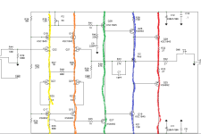
current through yellow=measure voltage across R35 and calculate current using ohm's law... should be ~2mA
current through orange=measure voltage across R37 and calculate current using ohm's law... should be ~2mA
current through green=measure voltage across R30 and calculate current using ohm's law... should be ~700uA
current through blue=measure voltage across R38 (or R31) and calculate current using ohm's law... should be ~10mA
current through red=measure voltage across R32 (or R33) and calculate current using ohm's law... should be ~12mA
I believe Wayne said each channel of the std. version draws ~25mA, so my numbers should be reasonably close.
DC current flows from one supply voltage rail to the other supply voltage rail in each of these legs when things are working properly. Hopefully I've stressed the importance of using ohm's law to figure out if current is flowing, and if it's the proper and expected amount.
Attachments
Try reconnecting the negative rail wire from your PSU.Following advice to check the SMDs, I hit them again with solder and got the right led up to the brightness of the left. But DC offset remained at 14.4v and still unaffected by the pot. When I made another pass at suspect joints, the led went back to its dim state and DC offset remained 14.4v. I previously got discouraged with this project and let it sit in my workshop, where it got pretty grungy, until I decided to give it another go. I’ve got a chassis that fits my Pete Millett balanced Nutube pre, so I was thinking I’d have a pretty simple swap of the boards and power supply.. Hasn’t worked out that way. But I’ll stick with it.
Last edited:
You're welcome. The whole shebang really relies on the input stage, also called the "IPS" (yellow and orange legs) to function properly to get everything else going. So the focus should be there first.Great info, thanks.
More good advice, thanks again. Let me ask about “pinging” the SMD legs — for continuity, I take it. I follow the schematic for the right trace and place my probe on a leg and a resistor leg? And that’s done with power off, I assume, while I do the current measures with power on?
@jfuquay: Yes that is correct. Do this first to ensure that the connections are being made. The first points are usually resistors but in some cases "Q" values. Is somewhat complicated for the right side of the board as only the left side is reflected by the schematic opposite the parts BoM. You can find this right side in early posts or extrapolate the connections by carryover from the left side (positions are inverted, sort of).
My experience has been that too much solder can hinder a SMD connection and, of course, you need to make sure that the leg and the PCB spot are properly heated before soldering. This will then float the solder on easily and the connection will be solid.
My experience has been that too much solder can hinder a SMD connection and, of course, you need to make sure that the leg and the PCB spot are properly heated before soldering. This will then float the solder on easily and the connection will be solid.
you guys are the most awesomest! Success on both channels. I didn’t think I’d ever get the SMDs right, but they fell into line. Seriously, I had all but abandoned this project. Thanks again.
- Home
- Amplifiers
- Pass Labs
- Wayne's BA 2018 linestage