
... Could you suggest a buffer design that I could try.
The M2x power amp has a "removable input stage daughter card" arrangement, allowing you to swap out and swap in nine different cards fairly easily. Each daughter card is a buffer, so those designs might be candidates.
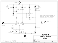
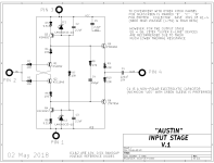
I doubt whether you would use the exact same PCBs for those buffers --- in the M2x design, the PCB mounting bolts are also electrical connectors (IN, +23VDC, OUT, -23VDC) . But you could certainly copy or copy-and-modify the circuit designs, and build them on whatever circuit board arrangement pleases you. Here are three examples; the rest are linked to from the first four or five posts in the M2x discussion thread.
_
Attachments
Well....by not being aware there was an issue
https://www.diyaudio.com/community/threads/waynes-ba-2018-linestage.329240/post-6453169
The M2x power amp has a "removable input stage daughter card" arrangement, allowing you to swap out and swap in nine different cards fairly easily. Each daughter card is a buffer, so those designs might be candidates.
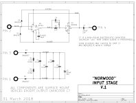
I doubt whether you would use the exact same PCBs for those buffers --- in the M2x design, the PCB mounting bolts are also electrical connectors (IN, +23VDC, OUT, -23VDC) . But you could certainly copy or copy-and-modify the circuit designs, and build them on whatever circuit board arrangement pleases you. Here are three examples; the rest are linked to from the first four or five posts in the M2x discussion thread.
_
XRK sells a tester board that is compatible with the M2X daughterboard format, so a buffer using the original boards could be built. But that seems like an unnecessary complication for a line level buffer. I think Andynor made very good suggestions in post#4728.
Regarding the C1 and C7 capacitors in the kit from the store, I guess the standard is the 10pF. Is the 5pF alternate used with the alternate transistors with the ability to drive headphones? If we choose to use the more powerful transistors, does that alter the sound of this unit? Thank you for answering my question.
Latest update, transparant smokey glass and bigger aluminium knobs.


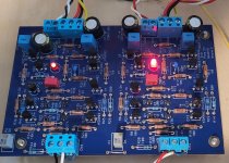
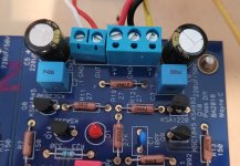
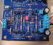
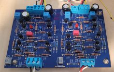
So I'm also building a BA2018 preamp (as opposed to headphone amp). I had installed Q11 backwards, which obviously was causing problems. I've now replaced it, but I'm seeing -17VDC (from a -18V supply) on the outputs. That's what would be biasing Q11. As you can see in the photos, the LED on that side is also very bright, because it's getting 17V. I thought maybe the other transistors nearby were fried, so I replaced Q8, then Q9 and Q13, but no effect. Any ideas? Photos attached.
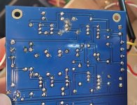
I am thinking the next step might be to replace all the transistors...or just start over. The back of the board is already becoming a bit of a mess from desoldering and resoldering.
I am thinking the next step might be to replace all the transistors...or just start over. The back of the board is already becoming a bit of a mess from desoldering and resoldering.
Attachments

I suggest you measure the voltage drop across R1, R2, R4, R5, R14, R15, R7, R13, R11, and R12 to see what currents are flowing and where the currents are flowing as a start.
I do not have this linestage and I am not familiar with it, but with that information perhaps something will stand out and someone will be able to help you.
I do not have this linestage and I am not familiar with it, but with that information perhaps something will stand out and someone will be able to help you.
You might want to check Q1 & Q2 and reflow the connections. Why does Q13 look burnt on the face of the transistor?
Every time I had close to rail voltage on the outputs, it was because Q1 - Q4 had poor connections.
Every time I had close to rail voltage on the outputs, it was because Q1 - Q4 had poor connections.
Can the Mean well LRS-150-24 be used to power the BA 2018 Linestage ? I did do a search but found no posts.
Not really, the 150-24 is a single supply, the BA2018 needs something bipolar, +/-15v to +/-24v.
Do what 6L6 said. But first, the easiest way of figuring out solder/continuity issues, is to measure resistance from point to point through the whole circuit. For example, put one dmm probe on the gate solder blob of q2, and the other probe at the next point in the circuit (a resistor leg I believe). Is the resistance close to 0R? If not, what happens when you press the JFET leg a bit with your probe? Just power it off, and play a bit. You’ll hack it. But with this circuit, fault is usually in the JFET soldering.So I'm also building a BA2018 preamp (as opposed to headphone amp). I had installed Q11 backwards, which obviously was causing problems. I've now replaced it, but I'm seeing -17VDC (from a -18V supply) on the outputs. That's what would be biasing Q11. As you can see in the photos, the LED on that side is also very bright, because it's getting 17V. I thought maybe the other transistors nearby were fried, so I replaced Q8, then Q9 and Q13, but no effect. Any ideas? Photos attached.
I am thinking the next step might be to replace all the transistors...or just start over. The back of the board is already becoming a bit of a mess from desoldering and resoldering.
This one at AmazonNot really, the 150-24 is a single supply, the BA2018 needs something bipolar, +/-15v to +/-24v.
https://www.amazon.com/LRS-150-24-Switching-Supply-Single-Output/dp/B018RE4CWW
does seem to have positive and negative outputs. Would you want some extra filtering with a switching supply?
- Home
- Amplifiers
- Pass Labs
- Wayne's BA 2018 linestage