Q10 is cold as ice compared to Q8.My poor eyesight, I meant Q10 on the schematic.
I would start by looking at Q5. 17.8V at the collector is the same as PS voltage, indicating no current is flowing.
I was meant to say both Q8 and Q10 is maybe happened to be NPN?Q8(Q20) happen to be NPN?
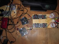
Boards look fine, like you did a good job.Anybody else has an idea based on the voltage on the schematic?
I think I’d start by verifying the JFET CCS works as it should. Did you do this or only resolder the joints? If you provide measurements of the voltage drops across R1-4, that will help. If all these are fine, look further down the line/circuit.
Also, Rainfallsky has a point: verify all bipolars are in the correct positions, very easy to mess that up.
I connected Q5 emitter and base pins in sim and have something like what e_fortier measured..I would start by looking at Q5. 17.8V at the collector is the same as PS voltage, indicating no current is flowing.
Sim go crazy if I connect Q6 B-E pins.
I connected Q5 emitter and base pins in sim and have something like what e_fortier measured..
Sim go crazy if I connect Q6 B-E pins.
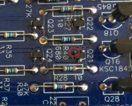
If so, the red circle might mark the spot.
Hi
I already checked the red circle and there’s no short.
I checked again, all bipolars are in the correct positions.
I have only resolder the 4 JFET
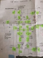
Attached is the updated schematic showing voltage around R1,R2,R4 and R5
Number on top is channel working ok.
Thanks everyone 👍
I already checked the red circle and there’s no short.
I checked again, all bipolars are in the correct positions.
I have only resolder the 4 JFET
Attached is the updated schematic showing voltage around R1,R2,R4 and R5
Number on top is channel working ok.
Thanks everyone 👍
Attachments
Last edited:
The solder joint on Q21 looks like a possible cold solder joint. I had the same issue. I replaced the JFETs and the problem was solved. Another time, I simply cleaned and reflowed. If I remember correctly, the SMDs are out of stock. When they come back into stock, I would order like 16-24 of them. They are very cheap and it is nice to have extras.
I would try cleaning the little JFETs with isopropyl alcohol to get rid of all of the flux, use a solder pen to reflow Q21 then report back. A buzz test with a multimeter should not be difficult. If it takes effort to get the tone, clean the SMD and your probe with isoprophyl alcohol, let dry and try again. If it is still difficult then the connection is suspect.
I would try cleaning the little JFETs with isopropyl alcohol to get rid of all of the flux, use a solder pen to reflow Q21 then report back. A buzz test with a multimeter should not be difficult. If it takes effort to get the tone, clean the SMD and your probe with isoprophyl alcohol, let dry and try again. If it is still difficult then the connection is suspect.
Attachments

Again, 17.8V at Q5 collector is not good. There is no current flowing through R6/P1. Check soldering at Q5, or perhaps Q5 is defective?
Or issue with Q1 since it is next in line?
Or issue with Q1 since it is next in line?
Agree with mikerodrig. Clean and reflow and then reclean Q1+2 on the bad chan. Then verify the joint with buzzer between all three legs of each JFET and the next/adjacent point on the board (most often resistor legs). When all is good, all will be goodHi
I already checked the red circle and there’s no short.
I checked again, all bipolars are in the correct positions.
I have only resolder the 4 JFET
Attached is the updated schematic showing voltage around R1,R2,R4 and R5
Number on top is channel working ok.
Thanks everyone 👍

If you wanna do it very tedious, check continuity (buzz) first to identify the culprit joint, then reflow, then clean, then check again.
I’d be vary about replacing the JFET unless it is confirmed broken. I replaced once, and damaged the board underneath the fet. My own fault of course, but nevertheless
 If you do, ensure it is from the same reel.
I agree. Once you are at it, reflow Q5 and get rid of that solder island.Again, 17.8V at Q5 collector is not good. There is no current flowing through R6/P1. Check soldering at Q5, or perhaps Q5 is defective?
Or issue with Q1 since it is next in line?
Everything is screwed up if those JFETs are out of line. One of them unstable, and offset will drift wildly and many times multiple of that read off R1-2.I think Mikerodrig27 coul be right.
If i disconnect source pin on Q1 then even Q5 behave like it did.
one if them not working at all, no current will flow where it should, imoe. Nice to see spice confirms the trend.
SOLVED!!
Thanks everyone for your amazing help.
As suggested I verified the continuity from Q21,Q22 and had 1 cold joint on Q22 🤪
Everything is now OK, dc offset was adjusted fine.
I also cleaned the pcb near all JFET.
Thanks!!
Eric
Thanks everyone for your amazing help.
As suggested I verified the continuity from Q21,Q22 and had 1 cold joint on Q22 🤪
Everything is now OK, dc offset was adjusted fine.
I also cleaned the pcb near all JFET.
Thanks!!
Eric
Nice work! Very good of you to provide detailed measurements. Goes to show - once again - that most issues with these boards seem to stem from JFET troubles. Hence we can conclude troubleshooting them first is a good start for all having issues.SOLVED!!
Thanks everyone for your amazing help.
As suggested I verified the continuity from Q21,Q22 and had 1 cold joint on Q22 🤪
Everything is now OK, dc offset was adjusted fine.
I also cleaned the pcb near all JFET.
Thanks!!
Eric
Hello WLS-builders,
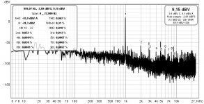
today I made my first measurements with my Focusrite Scarlett and REW on one of my
WLS-variants (variant3 = 2sk2394 ONSEMI JFets // 2N5551/2N5401 // output MosFets FQP3N30 /FQP3P20).
My signalgenerator from my Laptop puts out a sinus - signal (1 kHz) with a voltage swing of 0,068V (68mV).
Measured with my Fluke at the output (headphone out). Pretty low.
At the output of my WLS variant3 I have measured a voltage swing of 1,308 V AC at 1kHz (volume pot close to full volume). If I am hopefully right, this would equal a gainfactor of 19,23 or circa 25,6 dB.
Slightly higher 2nd harmonic distortion than 3rd.
Only some impressions. I hope I did not measure nonsense? 🤔
Cheers
Dirk 😉
Attachments

if measuring with Scarlet, it is logical that signal to amp is from Scarlet and measured signal is from amp back to Scarlet
so, what is meaning of "My signalgenerator from my Laptop"?
if you did use it simply for gain measurement, then OK
so, what is meaning of "My signalgenerator from my Laptop"?
if you did use it simply for gain measurement, then OK
- Home
- Amplifiers
- Pass Labs
- Wayne's BA 2018 linestage