Unfortunately I can't edit my above posting. I've done a negative version and tidied it up a little bit.


Nice nfs!
The pcb’s can be manufactured for a very reasonable cost by keeping the longest dimension 100mm or less.
I’ve built a few amps with remote mosfet mounting that had gate and snubber components close to mosfets without any oscillation issues.
I believe Mbrennwa built a very successful compact USSA5 with remote mounted LatFets.
That’ s right and even without snubbers!Nice nfs!
The pcb’s can be manufactured for a very reasonable cost by keeping the longest dimension 100mm or less.
I’ve built a few amps with remote mosfet mounting that had gate and snubber components close to mosfets without any oscillation issues.
I believe Mbrennwa built a very successful compact USSA5 with remote mounted LatFets.
Fab
Last edited:
Hi nfsgameUnfortunately I can't edit my above posting. I've done a negative version and tidied it up a little bit.
View attachment 1065196
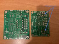
nice! A few comments if I may:
1) increase size of PSU caps to populate at least 2200uf (50v or 63v). You can move source resistors closer to the top if needed.
2) marking:
A)V+ is not connected to Drain but to R source. Drain of mosfet is connected to output. Same thing for V-.
B) it could be used for a wider range. Ex: USSA and FSSA Twin Turbo extension board….
3) adding extra through holes can be used for Lateral and also Vertical mosfet and BJT. See attached picture (on the right) of my USSA-4 Mini Pcb.
Fab
Attachments
So there is Rev 0.3!
Caps are 18mm/7.5mm now so they could be Nichicon UVR 2200uF/63V, UCC GPD 2400uF/63V or something fancy like Nichicon UKZ 1000uF/50V.
Pads for switching leads are included now, snubbers went to the bottom and are surface mount now. But no reason to worry - they are MELF respective 1206. I could solder them faster and more comfortable then classic through hole parts as there are no nasty leads to cut off ...
Markings are cleaned up to be more universal as a tribute to the lead switching pads and to avoid confusion.
@fab: I've sent you a DM regarding the schematics to check them with mine respecting the extension board part. Would be very nice if I could get them for that reason.
Really helpful, and glad you've allowed space for Nichicons (will Super throughs be possible?)... you can sign me up for PCBs (BLACK 🙂 ), if you reach that stage.So there is Rev 0.3!
Caps are 18mm/7.5mm now so they could be Nichicon UVR 2200uF/63V, UCC GPD 2400uF/63V or something fancy like Nichicon UKZ 1000uF/50V.
Pads for switching leads are included now, snubbers went to the bottom and are surface mount now. But no reason to worry - they are MELF respective 1206. I could solder them faster and more comfortable then classic through hole parts as there are no nasty leads to cut off ...
Markings are cleaned up to be more universal as a tribute to the lead switching pads and to avoid confusion.
@fab: I've sent you a DM regarding the schematics to check them with mine respecting the extension board part. Would be very nice if I could get them for that reason.
View attachment 1065394
Hopefully it will be easier to provide instructions for as well. I don't really understand the layout of the double die - I've not seen it done... I'm not that experienced.
With USSA 5.2 Twin Turbo, delivering some 130-140w into 4ohms, the current requirement has the potential to exceed 5Amps? I was considering using XRKs smooth like butta Cap Mx, but max output is 5A. So need a solution, e.g. additional Cap bank or stick with CLC/CRC?
I read that XRK struggled to achieved ripple under 5mA with traditional CLC, CRC solutions, which gives me a point of reference, so I'd like to attempt Cap-Mx if poss.
Thanks
Last edited:
22mm with 10mm pitch would be the maximum that fits limited at 100mm boardlength - and that's already very tight. But I don't know if it's going to be useful. The 1000uF/50V Super Through's I've got in my stash are having a really high ESR compared to their competitors in the "smaller" footprint - about 120mOhm. Also a 2200uF/63V 381LX with 22mm size and 10mm pitch has about 160mOhm ESR. They are simply made for another position in a circuit.will Super throughs be possible?
Thanks
Just to be clear,
Fab
- Turbo version stands for higher PSU voltage for more power and in class AB (at medium to high power). This is achieved by a single package pair ( N + P) of vertical mosfet or BJT or with a single pair of « double die » package of Lateral mosfet. Double die means 2 transistors in patallel in the same package. Therefore, a single pair of double die lateral mosfet is equivalent to 2 pairs of 2SK1058/J162. for example, you can make an USSA-5.2 Turbo running at +/- 45VDC in class AB ( with medium bias) with a single pair of double die lateral mosfet.
- Twin Turbo stands for 2 pairs of vertical or BJT or double die lateral mofset. The latter is equivalent to 4 pairs of 2SK1058/J162! This is for difficult speaker loads.
Fab
Thanks Fab - this is clear… but 🙂 … a relatively inexperienced person like myself (decent with a soldering iron and schematics, but no formal electronics background) doesn’t know:
1. Which examples of double die lateral mosfet are being suggested, is there a double die version of ECW20N20/20P20 for example?
2. The dual turbo helper board, literally helps with this, but how best do you place and connect the mosfets without this additional PCB? Looking for a practical example / photos.
Waiting for the USSA5.2 TT schematic, this would aid my understanding for sure. I’ll take any and all instructions that are offered 🙂
They are already double die versions of their * 10N*/* 10P* alternatives as far as I know...is there a double die version of ECW20N20/20P20 for example?
Oh it’s literally that simple! Thanks.
How are 4 pairs arranged on the board without the helper PCB?
How are 4 pairs arranged on the board without the helper PCB?
Two pairs, not four.
The double die is inside the TO247 case.
You just have to add wires in case of an additional pair
The double die is inside the TO247 case.
You just have to add wires in case of an additional pair
Yes sorry - so how do you arrange two pairs of ECW20N20/20P20 (which is a double die lateral mosfet) without the PCB helper?
Apologies for hogging up the thread, you guys might think this is easy.
Apologies for hogging up the thread, you guys might think this is easy.
One complementary pair is soldered to the amplifier pcb, the second complementary pair is attached to the heatsink and P2P wired to the amp pcb with the needed resistors and caps.
The helper boards come in Positive and Negative versions, a pair of P-channel Fets soldered to positive pcb and a pair of N-channel Fets soldered to the negative pcb. Then solder flying leads from each helper pcb to main amplifier pcb. No Fets are soldered to the main amp pcb.
The helper boards come in Positive and Negative versions, a pair of P-channel Fets soldered to positive pcb and a pair of N-channel Fets soldered to the negative pcb. Then solder flying leads from each helper pcb to main amplifier pcb. No Fets are soldered to the main amp pcb.
Think about the FET with his two resistors as one unit. This unit is doubled now. You will wire from the "entry point" of the gate resistor on the PCB to the "entry point" of the gate resistor of the extra unit. Also wire the "exit point" of the source resistor of the extra unit to the "exit point" of the source resistor on the PCB. The drains in this example don't have any special with it. So they are simply connected with each other using a piece of wire.
The gate resistor always have to be as close to the gate pin as possible to avoid instability. There are even commercial amplifiers on the marked where the manufacturer removed a piece of the FET pin to solder the gate resistor closer to the FET entry (take a closer look at the bigger accuphase models of the early 2000s).
The gate resistor always have to be as close to the gate pin as possible to avoid instability. There are even commercial amplifiers on the marked where the manufacturer removed a piece of the FET pin to solder the gate resistor closer to the FET entry (take a closer look at the bigger accuphase models of the early 2000s).
Last edited:
Thank you NFSgame! OK, I’m definitely waiting for the helper PCB board as I presume this will come with suggested gate resistor values depending upon FET used.
I’ll leave you to carry on the good work.
I’ll leave you to carry on the good work.
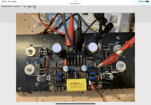
Here is what I have done for USSA-7 (FSSA pcb) and USSA-8 (USSA0cb) w/o the pcb helper.Yes sorry - so how do you arrange two pairs of ECW20N20/20P20 (which is a double die lateral mosfet) without the PCB helper?
Apologies for hogging up the thread, you guys might think this is easy.
Fab
Attachments

Rev 0.4 done...

- Removed snubbers until I've an idea how to place them without harming the current traces
- Current traces are now bigger and double-sided stichted-through for maximum surface area and best possible conductance
- Surfacemount pads for the big caps added as a reaction of the EOL-announcement of various TTH-cap series by Elna last week (RFS, ROA) and Nichicon today (UFW, UFG, UKL, UVR, UKW, ... 🙁) - one could now use Rubycon TRV 1500uf/50V or Vishay 146CTI 1000uf/50V or similar in the future when there is less choice for TTH-parts...
- Protection diodes added respecting fabs manual for the twin turbo versions
Last edited:
Do USSA7 & USSA8 also use FQP3P20/FQP3N30 same as USSA 5.2 Twin Turbo?
FQP3P20/FQP3N30 are about to go obsolete, but currently still decent stock at Mouser.
FQP3P20/FQP3N30 are about to go obsolete, but currently still decent stock at Mouser.
- Home
- Group Buys
- USSA-5 PCB GB