This is..... Interesting...
Dominic.. What ya think of it?
How many amps is this. I imagine is less than 1amp
Dominic.. What ya think of it?
How many amps is this. I imagine is less than 1amp
Last edited:
Hi Anthony,
I’m sure it will be another super nice amplifier from Fab but I have not yet heard it because of social distancing. We’re also not yet allowed to enter someone else’s house.
When I can, I will definitely take the USSA3b for a spin.
All the best!
Do
Btw, tried to email you but got a bounce back saying your inbox was full.
Oh no wonder ..
I think will be very interesting amp. Bipolar sounds more tubish than lat mosfet and have better low control . This should be a pretty nice class a amp .
If the depth / seperationis as good as exicon
It should be a winner
Very cleber godzilla
I think will be very interesting amp. Bipolar sounds more tubish than lat mosfet and have better low control . This should be a pretty nice class a amp .
If the depth / seperationis as good as exicon
It should be a winner
Very cleber godzilla
Last edited:
Fab,
starting to move this project. unfortunately no more 170 gr low gain.
possible if I use parallel the bipolar. a set of 2 will solve it?
because I'm using for 8 ohm jbl old school speakers
anthony
starting to move this project. unfortunately no more 170 gr low gain.
possible if I use parallel the bipolar. a set of 2 will solve it?
because I'm using for 8 ohm jbl old school speakers
anthony
Hi AnthonyA
If you cannot locate GR grade jfet then you can use lowish IDSS grade jfet (<= 8ma). Using 2 pairs of bipolar as outputs will not help that much since each one will have half the bias. I had not checked this avenue yet to increase the open loop gain….
If you want to use bjt for input then you must switch to USSA-5.x build as the bjt require current sources as opposed to jfet self biasing. In fact, the USSA-5 is the bjt input version of the USSA-3 and all USSA-3 and USSA-5 versions use the same pcb you have.
Let me know if you need the USSA-5.x manual.
Fab
Last edited:
I had not in mind that you were building USSA3B where jfet IDSS needs to be lower than USSA3 with mosfet output.
Still it should work fine with IDsS of 6.x ma but damping factor will be less…
See below expected DF on USSA3B based on input jfet IDSS:
IDSS= 3ma —> DF= 60
IDSS= 7ms —> DF= 30
Some ussa3.0 amplifiers were built with DF of about 25 to 30 with good reported sound.
You can interpolate DF value based on that.
Fab
Last edited:

hi Fab
what can you recomend for 8 ohm speakers
i rather go for optimal
knowing you... won't do it otherwise.
all your projects is reliable and excellent
Anthony
what can you recomend for 8 ohm speakers
i rather go for optimal
knowing you... won't do it otherwise.
all your projects is reliable and excellent
Anthony
Hi AnthonyA
For 8 ohms speakers a DF of 30 would be quite fine (but maybe not optimal for hard rock music depending on speakers 🙄). We can push DF a bit higher by increasing the driver current too.
There would also be another way to increase DF which consists in replacing the darlington bjt drivers complementary pair with a high VGSoff mosfet complementary pair readily available.🙂
This is what I am testing on the USSA-5.2 (new version). Bench tests are completed and listening test is on-going since last Saturday. I can adjust DF easily with the trim pots. Quite promising so far….
As for a new USSA-3.2B (mosfet drivers stated above) then I am not there yet but maybe on my to-do list…
it is just that USSA-5.x versions seem much more popular than USSA-3.x versions…🙄
Thanks for your appreciation of my projects, this alone justifies my hours taken to share and support these projects 🙂🙂
Fab
Last edited:
I should have clarified that damping factor is related to load impedance thus DF of 30 into 8 ohms translates into 15 into 4 ohms.
Fab
Fab
FAB ,
My apologizes if some issues pointed out here seem a bit trivial , or have already been answered ,
but I think there needs to be an FAQ section for people building the USSA 3 Amps .
Please point out if any corrections are required .
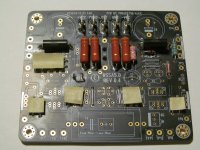
Building the USSA 3.2 Amp * ... on the USSA 5.0 Rev 4 board ,
1 ) The 4 ellipses on the schematic indicate that 4 jumpers are required .
As you've shown in Post #1 and I've shown in the photo attached .
Jumpers are required across R3 , R4 , C3 and C4 as well as RV2A and RV2B .
I set up a bar , to connect a scope probe ground , on the jumper of C3 .
2 ) It would not be happy moment if the jFET's got soldered into the wrong location
Q1 on the board - J1 2sk170 BL
Q2 on the board - J2 2sj74 BL
Q3 and Q4 are left empty .
3) As for the analog grounds , I'm still thinking about this
GC - low current analog ground , for the voltage gain section
This marked as Gnd right in the middle of the board ( right beside the USSA inking ) .
GP - high current analog ground
* USSA 3.2 Amp
2sk170 BL ===> FQP3p20 ===> ECW20p20
2sj74 BL ====> FQP3n30 ===> ECW20n20
.
My apologizes if some issues pointed out here seem a bit trivial , or have already been answered ,
but I think there needs to be an FAQ section for people building the USSA 3 Amps .
Please point out if any corrections are required .
Building the USSA 3.2 Amp * ... on the USSA 5.0 Rev 4 board ,
1 ) The 4 ellipses on the schematic indicate that 4 jumpers are required .
As you've shown in Post #1 and I've shown in the photo attached .
Jumpers are required across R3 , R4 , C3 and C4 as well as RV2A and RV2B .
I set up a bar , to connect a scope probe ground , on the jumper of C3 .
2 ) It would not be happy moment if the jFET's got soldered into the wrong location
Q1 on the board - J1 2sk170 BL
Q2 on the board - J2 2sj74 BL
Q3 and Q4 are left empty .
3) As for the analog grounds , I'm still thinking about this
GC - low current analog ground , for the voltage gain section
This marked as Gnd right in the middle of the board ( right beside the USSA inking ) .
GP - high current analog ground
* USSA 3.2 Amp
2sk170 BL ===> FQP3p20 ===> ECW20p20
2sj74 BL ====> FQP3n30 ===> ECW20n20
.
Attachments
OK so trying to understand how the analog grounds work
For an amplifier , there are small voltage drops across the cables .
So the RCA ground , speaker ground , amplifier ground and power supply ground
should all be referenced to a star ground node in the same physical location .
Everything is referenced to the same " 0 " Vdc .
Some people argue that the ground on the power supply is the quietest location in a circuit
so the star ground node should be on the power supply .
FAB shows this in his booklet as Option 1
Other people on this forum argue that its an amplifier ,
so the star ground node should be on the Amp Board itself .
So there are 2 star ground nodes one for the L and and the other for the R channel .
FAB shows this in his booklet as Option 2 .
I was thinking of putting the star ground node 1/2 way between all 4 items .
and having 2 star ground nodes one for the L and the other for the R channel .
Since the jFET's control the Vgs of the MOSFET's , I would have thought its important to
have them all referenced to the same Ground node .
So I'm still trying understand the need for GC - the low current ground and
GP - the high current ground separated by a small bit of resistance .
Use 12 awg wiring minimum , as FAB recommends for all high current wiring .
One trick - if the noise and ripple on the power rails , are equal but opposite in phase , and if Vout = 0 Vdc ,
then the ripple and noise should cancel each other out at Vout .
So for this reason , in my opinion , I'd say set the length of the +Ve and -Ve cables from the power supply ,
to the amp board , to be the same length .
.
UunderhillFAB ,
My apologizes if some issues pointed out here seem a bit trivial , or have already been answered ,
but I think there needs to be an FAQ section for people building the USSA 3 Amps .
Please point out if any corrections are required .
Building the USSA 3.2 Amp * ... on the USSA 5.0 Rev 4 board ,
1 ) The 4 ellipses on the schematic indicate that 4 jumpers are required .
As you've shown in Post #1 and I've shown in the photo attached .
Jumpers are required across R3 , R4 , C3 and C4 as well as RV2A and RV2B .
I set up a bar , to connect a scope probe ground , on the jumper of C3 .
2 ) It would not be happy moment if the jFET's got soldered into the wrong location
Q1 on the board - J1 2sk170 BL
Q2 on the board - J2 2sj74 BL
Q3 and Q4 are left empty .
3) As for the analog grounds , I'm still thinking about this
GC - low current analog ground , for the voltage gain section
This marked as Gnd right in the middle of the board ( right beside the USSA inking ) .
GP - high current analog ground
* USSA 3.2 Amp
2sk170 BL ===> FQP3p20 ===> ECW20p20
2sj74 BL ====> FQP3n30 ===> ECW20n20
.
this info is already in the USSA3 manual, except the use of the drivers you mentioned.
Fab
Fab , originally thought I would build FSSA -2 amp , so I ordered FSSA - V3.0 boards ,
so the manual sent looks to be for the FSSA - 2 Amp .
But I also ordered USSA 5.0 REV 0.4 boards . I know F5 style amps quite well , so have since decided to build the USSA 3.2 amp .
So I'm trying to figure out where the jumper wires go on the USSA 5.0 REV 0.4 board .
To add to the list above ,
- To connect P3 to Gnd , a jumper wire is required from R9 to the Gnd eyelet at the center of the board .
- R32 connected between Gate of J1 on the board to Fbk ??? ( Note : J1 on the board , not J1 of the circuit ) .
.
Uunderhill
all the jumpers info to adapt USSA 5 v0.4 board into USSA 3 build is part of the USSA3 build manual.
Fab
all the jumpers info to adapt USSA 5 v0.4 board into USSA 3 build is part of the USSA3 build manual.
Fab
So FAB , I'm coming into the home stretch of building the USSA 3.2 .
Have matched the 2sk170 and 2sj74 BL with an Idss between 6mA to 8mA , as provided by DIYAudio Stores
Have 4 of each as provided by Profusion , Exicon ECW20n20 and ECW20p20
In 2024 , I'm not even going to try to find the mythical 2sk2013Y and 2sj313Y 's .
But ... I have quite a number of FQP3n30's and FQP3p20's bought from Mouser and Newark , so I have every confidence they are real . *
For the FQP3n30's , Yfs ( typ) = 1.75 S ..... and FQP3p20 Yfs ( typ ) = 1.23 S .
Dumb Question # 58 , with the differences in Yfs , is there any point trying to match these ?
But ... I do plan on testing the amp with only the jFET's and the FQP3n30's and FQP3p20's to make sure all is well .
Running them at 25mA or 30mA
If all is well , then solder in the Exicon MOSFET's .
* I used to talk with a sales rep from ABRA . He told me he has seen a shipment of transistors where there was nothing in them .
They were just TO-92 plastic cases .
.
Hi Uundehill
if your transistors directly come from these big distributors then you cannot do better unless you bought them directly from the manufacturer -which might prove difficult for an individual, except for samples….
No need to match N with P channels. Try instead to have about similar Ns and similar Ps to have similar left and right amplifier channels.
25-30ma is low to get max performance from these transistor.
Testing methodology is explained in the build manual and must be followed. It is the best part of the manual and I support the builders who follow this manual step-by-step…
to-92 package is not for FQP but rather input jfet….😉
Fab
- Home
- Amplifiers
- Solid State
- USSA-3B new Version based on USSA-3