Then you are extremely fast at routing, it would take me a week what you did in a day.I guess your comment is directed towards Brian, but anyway, no - I don't use autorouter. I have tried it (looong time ago) and felt that there was litlle to gain. And much tidying-up during and after the process.
Hi Nico,
I do not use auto-router. I don't think its not a realistic tool for audio layouts. Routing is time consuming. This is just a hobby for me, so I'm not very efficient at it. The end result may be good, but it takes me awhile. Users that do this for a living like @prasi would likely come up with a much better layout in about a 1/10 of the time. I also always end up with vias to move traces between the top and bottom layers. Prasi's boards rarely have this - he is truly gifted.
I spend a lot of time on the ground routing as I feel this is an area that is often neglected. I use the approach that the Wolverine boards use.
My layout is oriented toward a chassis with side mounted heatsinks. I think my boards are too long for your approach. But if you think they'll work for you, send me a PM.

I generally don't like the hot-rod look with heat sinks on the sides. I think another alternative would be that of two heat sinks inside with input close to the back plate. I will do some fitting using pieces of paper since I have a box that I want to use. I think I showed in an earlier post. All that I have is time, so I will keep myself occupied for a while. I hate making things on the fly, it becomes too expensive. Unfortunately mistakes are costly because anything I do is per contract. I do not have the capabilities any longer to do what I like with my own hands.
Still I loved this thread and hope many would contact you for group buys and the like. Next time take my advice and make up kits for purchase directly, freebees are fine but time remains money.
Thanks for allowing me to post my thoughts on your thread, I thoroughly enjoyed it.
Still I loved this thread and hope many would contact you for group buys and the like. Next time take my advice and make up kits for purchase directly, freebees are fine but time remains money.
Thanks for allowing me to post my thoughts on your thread, I thoroughly enjoyed it.
🤣🤣By the way, it won't work, there are no fuses installed! 😡
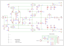
I'm about the send the new boards off for production and was doing a final review. Question for the Layout Experts on reducing ground loop area.
The V2+ trace is running on the top of the board. I think I can reroute this to run on the bottom along with the ground and V2- traces. I think this would reduce the ground loop area going to the IPS-VAS. Does this sound right? Is this something I should take care of before sending it off?

The V2+ trace is running on the top of the board. I think I can reroute this to run on the bottom along with the ground and V2- traces. I think this would reduce the ground loop area going to the IPS-VAS. Does this sound right? Is this something I should take care of before sending it off?
@Vunve, Board dimensions are 55mm x 240mm
Thank you for the kind words Nico. I put a lot of work into boards beyond just the basic layout. Like chassis compatibility, device footprints, and the top and bottom silk screen to aid builders. Nice to see it acknowledged.
Interesting thoughts on F81/F82. I did try to simulate different failure mechanisms, including one of the rails failing or the output being shorted. In those cases, the DC-DC converter current draw increased but did not exceed its limitations. One of the reasons I used the larger SIP8 devices is to allow enough dissipation to survive a fault condition. Perhaps the additional fuses are unnecessary. The board size probably won't change much though. Within the footprint for the fuse blocks F81 & F82 are connectors J81 & J82. These provide a pads for tab quick connects if the builder chooses to use an external V2 PSU. There is also jumpers JP80 & JP81. These allow a builder to omit the V2 PSU and provide power from the main rails. I can reorient these and maybe shave a few mm's off the board size, but not much.
View attachment 1363084
You wrote Gate diodes D92/92,94,91... do you mean diodes D94/95 and Zeners D92/93? These are not included in the Exicon to my knowledge. I thought it was D96/D97 that are redundant for the Exicons. As the datasheets don't seem to explicitly show the diodes, I thought it safer to add them as optional components. In either case, these are not necessary for the amp to function. A builder can choose to omit these. This is discussed in section 5.10 of the guide. Omitting D96/D97 has been brought up before. It wouldn't really affect the layout much, so I opted to leave them in as optional.
C13 and C14 may not be needed. Sims do not indicate they are needed, however many builders on this forum using Exicon laterals have indicated problems with oscillation in practice that don't show up in sims. I thought it safer to add them. When I assessed them in simulations, the impact on THD and slew was very small to non-existent. This is mentioned in the build guide in section 5.2.
R10/11 are recommended at 330R/220R for TO-247 and 220R/150R for TO-264. Similar to what you are recommending.
I have built several amplifiers with exicon lat mosfets. With 10P and 10N I always had oscillation problems if I didn't put C13 and C14. In the first few times I set 100pF but later I verified that 47pF is enough and the amplifier appears "less slowed down".
Curiously, with 20P and 20N I never had those problems and it was never necessary to add c13 and c14.
Hi adiaz,
Yes C13/14 have been a point of long discussions. I did remove the from the schematic. However, the boards did not have pads for them. They mounted into the pads of the MOSFETs in the original PCB. If they end up being needed, they can easily be added back.
My plan was to build with the new boards without them and check for any hints of oscillation. If needed, I'll add them back starting with a lower values.
Here's a picture of how they were implemented on the original boards.
Updated boards are in production. Now I need to work on getting the build guide and BOM updated.
Yep - 1W is not the issue. The transients where power levels will spike are the "issue". But this largely depends on how high your nominal listening level is. 1W nominal with a 14dB crest factor reaches 5W at the peaks. Which coincidently is just below the 5.75W Class A region with 600mA of bias 🙂.
This is probably where many will operate with efficient speakers... assuming you care about your hearing.
This is not correct.
Crest factor (CF) is the ratio between the peak amplitude (voltage) of the waveform and the RMS-value.
Peak-to-Average Power Ratio (PAPR) is the ratio between the square of these voltages, which is CF squared.
Expressed in dB, however, CF and PAPR are the same due to the way decibels are calculated for voltage and power.
Example:
Vrms = 2 V
Vpeak = 10 V
Hence, CF = Vpeak/Vrms = 10/2 = 5. This is equivalent to 13.98 dB, as CF[dB] = 20*log(CF).
PAPR = Ppeak/Pave = Vpeak^2/Vrms^2 = 10^2/2^2 = 100/4 = 25. This is also equivalent to 13.98 dB, as PAPR[dB] = 10*log(PAPR)
This means that if the average power (Pave) is 1W, then the peak power (Ppeak) is 25 W for CF = 5.
You can also see it this way. Let's assume a nominal impedance (Znom) - or rather a resistive load - of 4 ohm. This gives us:
Pave = Vrms^2/Znom = 2^2/4 = 1 W
Ppeak = Vpeak^2/Znom = 10^2/4 = 25 W
An overdue update:
I put the boards into production, but canceled. This was after finding a few things in simulations.
In addition to the amplifier, I'm working on:
I put the boards into production, but canceled. This was after finding a few things in simulations.
- The IPS rails now connect to the VAS emitters. This reduces high frequency distortion resulting in a 5dB to 6dB reduction in IMD.
- The input gate stopper has been split into two 1K resistors. This provides a small reduction in high frequency distortion.
- Anti-Saturation diodes have been added to the VAS. This provides a small improvement in clipping behavior. It might be more pronounced in real life. I understand that the models for SC3503/SA1381 don't model quasi-saturation well. These can be left unpopulated if the builder chooses.
- The bias trimmer VR3 now has a resistor in parallel. I found that when shorting the outputs, dissipation pulses were high enough to potentially cause failure of the trimmer. Paralleling with a resistor reduces dissipation across it and also allows the bias to be adjusted with greater sensitivity.
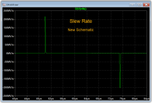
- Compensation has been changed to input-inclusive compensation. This requires fewer parts, has very similar THD performance and improves slew rate. It also has a lower ULG frequency for the same gain margins.
- The values for the MOSFET gate stoppers have been updated. I don't fully understand this one. By lowering the value of the P channel gate stopper, negative slew rate improves. High frequency distortion also drops. The resulting pole in the P channel MOSFET is still lower than the ULG frequency, so I think this is safe.
- One of the unused pins on the protection connector has been used to add a connector for a relay. This connector will placed next to the input connector. This makes wiring a bit cleaner if the protection board is at the front of the chassis and the output relay is at the rear. I attached a sketch of how I envision the chassis to be laid out with these boards in a dual mono configuration.
- The changes allow for the C1 input cap to increase back to a 37.5mm pitch footprint.
In addition to the amplifier, I'm working on:
- PSU with controls. This supports a dual mono CRC PSU with switch driver, 12V trigger, soft start, thermal switch and mains DC blocker. Design is complete and tested with breadboard. Boards are done. Working on a test build. The mains DC blocker is based on Bonsai's design.
- Output SSR board. Design is complete. Boards are done. Working on a test build.
- Protection circuits. This will include clipping detection, thermal protection (works with the PSU to disengage Mains relays), and DC Offset protection. These are based on Rod Elliott and Bob Cordell circuits. Still working on the design and breadboard testing. Boards will include indicator LEDs and will mount to the front panel.
Attachments


@brian92fs did you build the version with the IS fed from the VAS emitters?
For me that change causes instability in simulation with KSA1381/KSC3503. If I use TTA004B/TTC004B it is stable, but THD at 10kHz is twice as with the original circuit (both variants biased to 600mA bias through power MOSFETs).
For me that change causes instability in simulation with KSA1381/KSC3503. If I use TTA004B/TTC004B it is stable, but THD at 10kHz is twice as with the original circuit (both variants biased to 600mA bias through power MOSFETs).
What do you mean by instability? Loop gain analysis, square wave response, capacitive loading or something else?
It has not been built yet. I'm about to place the PCB order though. I'm using the same models and approach as the original, and it performed on the bench very close to what the sims predicted.
I attached my latest asc sim files if you'd like to take a look. These are currently set to run a 10kHz square wave at 25W.
Attachments
I definitely do, thanks.I attached my latest asc sim files if you'd like to take a look.
What I called "instability" is Spice having problems with doing reasonably sized steps in the simulation. That often happens if there is high frequency noise produced during simulating. According to my understanding, it can be caused by unideal models, missing parasitic resistance in the models (like for big capacitors etc.), using models of fast OpAmps, esp. the TI models cause this for me often. Or of course, it can be because there really is a prob.
In this relatively simple circuit, changing to connecting the IS to the VAS emitters was the only situation so far, in which my
This is not necessarily saying anything about real world, but it is irritating, I think. I will check which models you used and if it is not happing with them.
Another comment more related to my test build and the weird sine defect I had posted in lineup's thread: You are using LSK489B and LSJ689B and 1.2mA now. My real devices are more C band versions and as I wrote in the other thread, such a low IS current per device is very likely the cause of that deformation. I will verify that on my test build this afternoon.
I don't think the IPS current is all that important. I've tinkered with different values in sims, and it made little difference. If anything, performance degraded a bit at higher values. I choose 1mA because higher didn't seem to matter and lower allows the IPS to run cooler.
This design is similar to Bob Cordell's DH-220C. I see the Ultra as a simplified version of it. If you look at the paper on Bob Cordell's site, "Complementary JFET Offset Mismatch" there is a section where he states:
Now, this design is different from the DH-220C so this statement make not translate, but simulations seem to support it. My bench testing did not reveal any issues with the 1mA current. However, I have not bench tested higher IPS currents.
I also have not tried swapping in different grades of JFETs. I have a stock of Idss values from 3mA to 8mA. I plan to do this when I build version 2 too see if it has any impact.
This design is similar to Bob Cordell's DH-220C. I see the Ultra as a simplified version of it. If you look at the paper on Bob Cordell's site, "Complementary JFET Offset Mismatch" there is a section where he states:
Although the nominal IPS tail current is recommended to be set to 4.0 mA during the amplifier adjustment procedure, the truth of the matter is that the 4.0-mA number is a bit arbitrary, and amplifier performance is quite tolerant of minor changes in this current as long as the VAS bias current ends up within its fairly broad recommended range.
Now, this design is different from the DH-220C so this statement make not translate, but simulations seem to support it. My bench testing did not reveal any issues with the 1mA current. However, I have not bench tested higher IPS currents.
I also have not tried swapping in different grades of JFETs. I have a stock of Idss values from 3mA to 8mA. I plan to do this when I build version 2 too see if it has any impact.
I thought so too. When simulating I missed to see these small defects when lowering the IS current to about 1mA. See https://www.diyaudio.com/community/...ut-and-lateral-mosfet-out.409798/post-7833186 and following.I don't think the IPS current is all that important.
This is not theoretical. I measured it first and then when again looking closely at my latest sims, it was there too until I raised the IS current again.
Which schematic are you building against? I checked my sims and don't see any indication of that crossover artifact. I'm looking at the output when assessing this. Is this where you are looking? What frequency and amplitude are you observing it?
I can test my build on the bench against the same parameters that you are seeing it. My bench build is my original version still posted in Post #1.
I can test my build on the bench against the same parameters that you are seeing it. My bench build is my original version still posted in Post #1.
- Home
- Amplifiers
- Solid State
- Ultra Amplifier Build Thread