I accept your simulations Brian, I am referring to actual experience with these components, but if you want to be certain then that is of course your design. There can never be too much protection in anything.
This sums up my thoughts for C3/14. Sims say they are not needed. Experience from other builders say these may be needed in real-life. I only have an old analog scope and do not have a spectrum analyzer. I also cannot test every device combination and gain combination. So I choose to error on the cautious side and recommend them - especially when sims suggest they do little to no harm. Individual builder as free to do whatever they like.
I understand that being cautious can mean more components and a higher price tag to build. I've tried to explain my approach in the build guide if a builder wants to construction a minimalistic version. For example, all the 90 series components are optional. The amp will function without them. And the PCBs support building the amp without the V2 PSU if the builder wants to keep is simpler.
I take a similar approach to loop gain stability. Literature says 10dB and 45 degrees of margin is needed for stability. I aim for a minimum of 20dB and 65 degrees to be on the safe side. As well as keeping the bandwidth reasonable.

However, commercial ventures can also use a single BOM and have greater resources to test. And they will likely have a single approach to construction and a QA process (hopefully).
As a DIY project, we need to account for a wide range of components and build practices. We need to assume builders will make mistakes and try to come up with a design that is forgiving of errors. It's a tall order. It's the difference between a design & PCB for your own personal use vs designing for community use.
R3 is an example if this. It's technically not necessary. VR1 can simply be larger. But if a builder set the pot the wrong direction on initial-power on, they stand a good chance of frying the expensive JFETs or VAS devices. R3 mitigates this.
I added R14/15 for similar reasons. The adjustment for DC offset from VR2 should be small. But the original design allowed for a wide range of adjustments. While this may NULL DC, it will likely greatly compromise performance if the adjustment is excessive. It also means there is likely a problem elsewhere that the adjustment would be hiding.
Last edited:
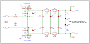
Here's what I'm thinking after incorporating Vunce and Nicos' input. The fuse blocks are removed and a PTC Resettable Fuse has been added to the positive rail.
As I examined this further, the intent of the fuse is to protect the DC-DC converters and these source from the positive rail. So, the fuse is really only needed on the positive rail.
I have it spec'd as optional (90 series). Its a 250ma / 500mA part. Meaning a 250ma holding current (125mA per rail) and a 500mA trip current (250mA per rail). The 250mA per rail correlates to DC-DC converter max current rating of 250mA. The DC-DC converters should draw about 35mA each in normal use and maybe 100mA of surge at startup. Even if the surge is higher the part has a 2+ second trip time, so they should survive any momentary startup surges.
I decided to leave the board size at 240mm x 55mm and provide a bit more space around the connectors. It was pretty tight before.
Attachments

I emailed Exicon to get clarification on what integral protection features they have:
That provides a bit of clarity hopefully.
The MOSFET’s have a back-to-back gate-source Zener diodes rated at 14v and also an integral body diode.
That provides a bit of clarity hopefully.
Fantastic work you’ve done here Brian, Sweet!
Yup, keeping the same dimensions without the fuse holders to free up space around the fastons for chunky finger room is a good idea.
Maybe ‘sleep on it’ tonight 😂.

Yup, keeping the same dimensions without the fuse holders to free up space around the fastons for chunky finger room is a good idea.
Maybe ‘sleep on it’ tonight 😂.
After much discussion in this thread and the original design thread, I'm thinking of a few changes:
Anyone have any sentiments against these changes?

- Increase R6 & R7 by a factor or 10. This will reduce the size of these resistors to 1/4W components. This allows C2 to be lower value and therefore use a higher voltage cap. With these changes, the anti-parallel diodes D90/91 are no longer needed. Discuss on this start at post #212 in the original thread.
- Remove the Gate-Source diodes D92 - D95. These are redundant to the Exicon devices integral protection.
- Remove D96/97. These are also redundant to the Exicon devices integral protection.
Anyone have any sentiments against these changes?
A lot of discussion going on in the original design thread about VAS currents and VAS degeneration. As a result, I'm rethinking some of the component values.
VAS degeneration R8/9 have been lowered which also lowers R4/R5. Performance improves, with the tradeoff of more variance in the OPS from cold to hot states. Still reasonable though. Maybe 50mA or 60mA of variance at most.
I also introduced lead compensation via C15 which lowers C3/4. This improves THD a bit, but increases bandwidth from 2.3 MHz to 4.3MHz. Not sure that this is good. We'd need to build it to see if this causes problems in practice.
This also incorporates the changes from post 128 above.
The schematic below has values for 2SC3503E / 2SA1381E. If TTC004B/TTA004B are used, R4/5 drops to 1K and C3/C4 are omitted. Perform will be similar with a slight nod to SC3503 /SC1381
And the layout updates. Board size remains the same, just more space around components. Which will be nice. Some of the Test Points were a bit tight in the original layout.


One other note... I revisited a Capacitance Multiplier vs the simple RCRC filter. The resulting PSRR was about the same. Only real upside to the Cap Multiplier is that it dropped less voltage allowing the MOSFETs to swing closer to the rails. You could theoretically run lower voltages for the same output and have less Class A dissipation. The additional complexity didn't seem worth it too me.
I am blown away by your PCB layout, it is beautiful! And I am not trying to suck up to you. Unfortunately, the other thread is getting a little overly complex and I think it is losing its original intention..
I plan to put the order in this weekend for the next batch of boards. I will send boards to anyone who recently purchased the original boards.
If anyone else is interested, please PM me so I can adjust the order quantity.
Thanks!
If anyone else is interested, please PM me so I can adjust the order quantity.
Thanks!
240mm x 55mm. I used this size to make it easier to fit on a heatsink as small as 2U. It should work work with the Modushop Dissipante 2U chassis and clear their mounting brackets.
Trying to get the build guide updated with all the changes, including dimensions and drilling. May take awhile longer.
Trying to get the build guide updated with all the changes, including dimensions and drilling. May take awhile longer.
Vunce, Brian is going to get a big head from all the praises. Just joking! He deserves the praise taking it all the way. Very nice thread.

Hahaha!!
All good and well deserved. My head is not big enough to deliver a complete project such as this. I appreciate the many “Big Heads” on this forum 🙂.
All good and well deserved. My head is not big enough to deliver a complete project such as this. I appreciate the many “Big Heads” on this forum 🙂.
- Home
- Amplifiers
- Solid State
- Ultra Amplifier Build Thread