Thanks Andrew, I always test in stages, systematically wiring and powering up the project in stages. To date I've used current limiting resistors but will give the light bulb tester a go - as you suggest.
Powered up...
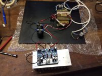
OK - I turned it on this morning after putting a 150R wirewound in each fuse holder and setting the trimpots to initial values. No smoke or fireworks so off to a good start 😀
Fuses went back in after a few voltage readings. Output DC offset is about -680mV which doesn't seem right.
Once warmed up the bias was set to 50mV and held stable.
Tried to bring the DC offset down by fiddling with the trimmer but it only made a few mV difference at either extreme of the trimmer. Q4 gets very hot when there is a lot of voltage at the Vbe emitter!
The measured voltage at the Q7 driver base doesn't seem right. Q6 and Q7 measure 69mV and -1260mV, respectively.
-V = 31V
after R15 (3k9 1W) the voltage is -16.4V
and after R14 (3k9 SMT) it drops to -1.26 (same as driver base)
I went over the board double checking everything and measuring all the resistor values. Seems right. Any ideas?
I'm tempted to plug in an old speaker and give it a go. 680mV isn't dangerously high but I would expect less.
Attachments
Last edited:
Member
Joined 2009
Paid Member
OOPs, this is a design fault - which idiot designed this amplifier ? 😱
The evidence suggests that the dc-offset adjustment runs out of compliance range when you build the simple (single transistor) VAS. I should have simulated the simple version to check this but I didn't. The issue is that I didn't design the circuit so that both options result in the same current flow through the input device and this affects the range over which the dc adjust works. But it can be fixed without any surgery.
In this topology, in terms of dc-operating points you want the base of the input device at zero volts and the amplifier output at zero volts. The emitter of the input device must be negative with respect to the base in order to keep the device turned on. Say -0.7V. Since this voltage appears on one end of the feedback resistor (R10) whilst the other end is at zero (dc-operating point) there is a current flow. This current, plus that flowing through the input device, has to flow out through the dc adjust circuit to the negative rail.
The way I have it now, the dc adjust circuit runs out of range when asked to sink the extra current flowing when the simple VAS is built.
The QUICK & SIMPLE fix is to replace the input device collector load resistor, R9, with a 1k resistor. This will drop the current through the input device to roughly the same value it would have with the two-device VAS and allow the dc-adjust circuit to work.
I'd like not to have to change the circuit values that were chosen by Rod, i.e. I'd prefer to be able to use 560R for R9 so I'll come back and visit this and possibly offer an alternative fix with some value changes that gives it a wider range of operation and is therefore more robust. With a 1k collector load the open loop gain will be a bit higher than Rod's baseline circuit but I don't think it will prove to be at all detrimental.
I suggest you do this quick fix and adjust out the dc-offset before moving on, it's way too much and the circuit will not have the operating points intended. When you fix it, the voltages at the drivers will all be sorted out.
Not surprising that the VAS warms up when given some big voltages to deal with. If you plan to use it at voltages where it gets warmer than you are comfortable with then I suggest fixing a simple DIY heatsink to it, bolt on a piece of metal such as some copper or aluminium. I tried to position the device on the pcb with 2mm-3mm of space for this. The trick with a little heatsink like this is to maximize surface area - be creative! Your measurements of the voltage drop across R15 allow you to calculate that the current flowing through this resistor is around 3.9mA - seems reasonable.
By the way, my boards arrived today !!!! - but my day job prevented me from placing my parts order. I've been so busy - just got back from travel to Montreal and Boston. I'll be placing an order soon. I may have most of the parts already in my junk box and may be able to put together something all the same with what I have.
Last edited:
Member
Joined 2009
Paid Member
If we want to keep R9 unchanged, the other option is to reduce the value of R12. You can avoid having to buy another value or remove the existing R12 by soldering a 27k (you have those for R2) on top of and in parallel with the existing 4k7 that you installed for R12. This changes R12 to around 4k which brings the dc adjust back into range and should work with both the simple and two-device VAS.
Happy soldering 😎
Happy soldering 😎
Member
Joined 2009
Paid Member
Member
Joined 2009
Paid Member
No that won't help - noticed I had a higher value feedback resistor (for more gain in the higher power version) so have re-run the simulation.
I've changed the values of R6, R11 and R12 - all these values are used somewhere so they'll be in your collection of parts. R6 drops to 750R, R11 drops to 1k5 and R12 to 3k3. This should restore some headroom for adjustments.
I've changed the values of R6, R11 and R12 - all these values are used somewhere so they'll be in your collection of parts. R6 drops to 750R, R11 drops to 1k5 and R12 to 3k3. This should restore some headroom for adjustments.
Attachments
Last edited:
Member
Joined 2009
Paid Member
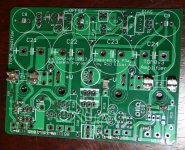
I started to build. No way I can get as neat a result as Ranchu32. Actually I notice that my solder has more surface tension, tends to ball up and make it harder to apply small amount than I thought it would. Well it's a excuse !
I don't have enough parts in my junk box to complete the assembly - my parts order is going out today and should have them in a few days.
I don't have enough parts in my junk box to complete the assembly - my parts order is going out today and should have them in a few days.
Attachments

I don't know what you're talking about Bigun, that soldering looks every bit as good as mine! Although I must say I prefer the blue boards to these green ones 😉 Please send me your address so I can mail a couple to you.
I made the changes you suggested in #206 (and changed R9 back to 560R) and it has improved the Vbe adjustment range considerably. I don't have any 1k2 SMT resistors so I've had to leave R10 at 1k5. I don't think that will have a large bearing on things and I'm reading around -0.9V at Q1 emitter now.
The other positive is that previously I was seeing significant (approx. -250mV) DC offset at the input. This has now reduced to low double digit -mV figures.
Although the voltages around the circuit are improved, I'm still getting a -ve voltage at the base of +ve driver.
My biggest drama is that as I adjust the Vbe trimpot to bring the voltage down at Q2 emitter, I can only get to about -4V before the VAS overheats and goes into thermal runaway. I've replaced the VAS once to ensure proper operation. I could try mounting a heatsink to the VAS but assume something is awry since it shouldn't be getting hot a quiescent operating conditions.
My reasons for these initial trials with low voltages are intentional: I wanted to test the "low power" with at both extremes. Once we've got the part values sorted I'll test operation with a 60VCT transformer.
Last edited:
Ranch - did you get a reply from qusp re the test gear? Also, let me know if you have any spare boards and are willing to send one down to me (I am in Adelaide). I can fix you up for the cost via paypal.
Hi lordearl
I never got a reply from qusp unfortunately. It would be great to have an experienced set of eyes to look at this - its a good thing Bigun's boards have arrived and he's making progress.
I'll send you a PM for the board details.
I never got a reply from qusp unfortunately. It would be great to have an experienced set of eyes to look at this - its a good thing Bigun's boards have arrived and he's making progress.
I'll send you a PM for the board details.
Member
Joined 2009
Paid Member
I agree, blue are best but don't send any - first we have to confirm this design is to our satisfaction before we call it final.... I prefer the blue boards ...I can mail a couple to you.
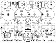
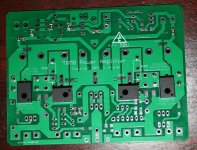
Lesson 1 - we found different rail voltages need different resistor values in the dc-offset circuit (perhaps one day I could redesign it to be independent of rail voltage). R10 is the feedback resistor, it is through-hole not SMT. The part names are hard to read off the pcb, check the parts-placement images in post #207; sorry for not posting them earlier....improved the Vbe adjustment range ... I don't have any 1k2 SMT resistors so I've had to leave R10 at 1k5.
Yes, something is awry- please check the part numbers you refer to in your description and write it differently as I am unsure what you are saying?I'm still getting a -ve voltage at the base of +ve driver... the VAS overheats ...something is awry.
VR1&Q2 are part of the dc-offset adjust circuit (the topology is a Vbe multiplier but this name may confuse with VR2&Q5). The only purpose of VR1 is to zero the output dc-bias, not to try and hit a particular Q2 emitter voltage. If Q2 emitter voltage is way off from the simulation this is useful information to understand what else is going on.
VR2&Q5 are the traditional "Vbe multiplier" to set the bias curent for the output.
The VAS should not be able to enter thermal runaway because the circuit controls the current through the VAS. Here's how. The current flow through the VAS is more or less determined by the resistors R14 & R15 in series. One end of this resistor chain is at -V the other will be close to zero (with no signal) so the current is i=31V/(3k9+3k9) = approx. 4mA.
Suppose for some reason (e.g. heating) the VAS (Q4) starts drawing more than this 4mA. In order to pull more than 4mA through R14&R15 it has to increase the voltage across this resistor chain. To do this the collector voltage of the VAS increases towards the +ve rail. The collector voltage of the VAS is connected to the amplifier output (via the CFP output buffers) so this change will be translated to the amplifier output. The negative-feedback network will feed this voltage change (error signal) to the emitter of Q1 (the 'error amplifier'), thus reducing the emitter-base voltage of Q1 and thus reducing the current though Q1 and through R9. This reduces the voltage drop across R9 and hence reduces the voltage presented across the base-emitter of Q4. This reduces the current through the VAS and thus opposes & corrects the heat-induced increase in VAS current we started with.
In this way the negative fdbk network stabilizes the dc-conditions for the VAS current set by the resistor chain forming the VAS collector load (in this case R14 & R15).
If you can tell me more about what is happening I can work out what the issue is. We need to fix the dc operating conditions before it's worth the effort of getting an oscilloscope hooked up.
I hope this is fun 😀
Last edited:
Member
Joined 2009
Paid Member
Further thoughts:
If the base of the +ve driver, Q6, is at a negative voltage and if the fdbk network is working as described then it will try to correct this negative offset by turning up the current flow through Q4. There is no limit as to how hard the feedback loop will try to fix this and it would result in huge current flow through Q4 - it would be capable of destroying Q4 easily.
If this is what is happeing then this excess current, which is flowing from the power supply via the +ve rail, through Q4 and out of it's collector must be going somewhere and it must end up back at the power supply through gnd or the -ve rail (or both). Assuming the schematic & pcb is correct we can think of some options to try and hunt down the problem by considering what is connected to Q4 collector.
a) Can the excess VAS current flow through the base-stopper, R17, into Q6 base ? - measure the voltage drop across R17 to see how much current is flowing through it. Under normal conditions the input impedance of Q6 is fairly high, the base will draw about 1/100th of the current flowing through the collector-emitter which under dc-operating conditions will be a few mA. The base current should be 10's of uA and the voltage drop across R17 in the mV range. If Q6 is turned-off you'll see next to nothing across R17.
b) Did you install R8, this is another place for current to flow from the VAS collector. Under normal conditions it should have roughly 1V across it and the current should be uA.
c) How much current is flowing through the other base-stopper, R16, into base of Q7 ? If Q7 is pulling a lot of base current then it's flowing a lot of emitter-to-collector current. This current has to find its way to the -ve rail through R23 or R27 so measure the voltage drops across them.
d) The only other place the current can flow is through R14&R15 - check the voltage drop across them too.
A wrong pin-out could be the cause, either from an error in the pcb, a fake part, or an error in installation.
Well, you get the idea, know where the current is flowing.
Last edited:
Thanks Bigun. I haven't and won't have much time over the next few days to play with this (work, baby, house renos) but hope to dedicate some "quality time" later in the week to work out precisely what's going on.
I think I've found the problem and I sure feel like an idiot...
Can you confirm the proper value of R7? I have a 0R resistor installed and I suspect there should be none.
Can you confirm the proper value of R7? I have a 0R resistor installed and I suspect there should be none.
IT PLAYS MUSIC!!
Curiosity got the better of me so I checked Rod's schematic and sure enough - no ground resister at the miller cap.
So I removed R7, plugged it in, adjusted the speaker out offset, which was now easily to dial into 0.00VDC.
Plugged an iPod and speaker in and it plays crystal clear music.
Off to see my family for Xmas but thought you'd like an update 😀
Member
Joined 2009
Paid Member
Fantastic - and just in time for Christmas 

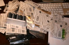
hey - my digikey order just showed up at my door too 😀
hey - my digikey order just showed up at my door too 😀
Attachments
Last edited:
Any updates Bigun? It's hard to resist posting photos of my second TGM8 board, complete with DC protection circuit, when I know you haven't even got your first one working yet 😀 
Any reason why you specify an output inductor for your design? Rod doesn't and I haven't noticed any ill effects without the inductor on your design.
Any reason why you specify an output inductor for your design? Rod doesn't and I haven't noticed any ill effects without the inductor on your design.
Any reason why you specify an output inductor for your design? Rod doesn't and I haven't noticed any ill effects without the inductor on your design.
If you are sure that your amp will never be exposed to any provocation in the form of capacitive loads, like electrostatic loudspeakers or high capacitance loudspeaker cables, you do not need it. But, I remember when my friend used two runs of 2,5m Kimber 4TC loudspeaker cables (for biwire) with Audiolab 8000 integrated (very good amp but without output inductor), it was enough to cause oscillation, overheating and triggering of output mute relay.
- Home
- Amplifiers
- Solid State
- TGM8 - my best amplifier, incredible bass, clear highs, no fatigue (inspired by Rod Elliot P3a)