I'm sure you was ! I am green country side pilgrimming next week but still connected, but no mobile workshop, ahaha !
Ciao, good holyday to you and to you all if having some.
Ciao, good holyday to you and to you all if having some.
hum forget the agnd to dgnd ic pins to planes conection I asked above in order to make it quiter between digital and analog part of the dac chip.
It's HF so it's obvious the current flows through the least impedance/inductance path, so will spread to the most adjacent layer of the digital pin connected plane.
Maybe better just to connect each pin where it belongs directly 3D (back to back diodes or wire if used between them, tht cap 3D connection above the ic (antenna?)) if at the next power pin of the ic. Illustration: DGND to 5V with a cap.
I was naivly thinking enlarging the loop between the two pins will lower the stray capacitance and also because the added inductance (despite being low cause one plain layer used just for each pin before they meet to the starground for the classic method with as last layer of the star ground vias a plain Vref layer) acheives some filtering of HF digital towards the AGND pin. But it would just enlarge the loop. So better to connect them near the "true" Ref (-15V/+5V...).
Questions of agnd/dgnd pins has been solved in the other long thread (posts of Thorsten and Zoran)
Last edited:

No surmising Iggy just for experience sake try out 25 vs 50v KZ. For 1 moment leave the inductance etc thoughts out & give it a gd listen.Inductance, won by the 25V/50V VS the 100V (for UKZ for whom who like it) due to the non usual bigger space pin of the 100V at Nichicon.
UKLs have of course very low leakage but even lowest inductance choice. I surmise we have to choose the UKL 16V cause in 10V the first value is 150 uF. A pity we have not more value choice at 10V (DEM is 7V around with normal conf, then T. gave the V values with its screen cap by cap DEM pin.
Edit : Hey George, thanks, I believed you was in holyday, had you have time to populate ? (PM)
big surprise ya. Specs are just specs you should know better. Oh dont remove the 0.1 uf pps caps.
Cheers
bad idea not to remove it ! No 50 hz for me until a board with a corect layout, not my priority yet.
I do not like ceramic, but wonder if some "no flex" treated amagnetic X7R will works (TDK ?) ? in lieu of the UKLs for you (in spite of the 0.1 PPS), what value and cap stylle do you use btw for the DEM C. (between pin 16/17) ?
I do not like ceramic, but wonder if some "no flex" treated amagnetic X7R will works (TDK ?) ? in lieu of the UKLs for you (in spite of the 0.1 PPS), what value and cap stylle do you use btw for the DEM C. (between pin 16/17) ?
Last edited:
Philips grading process at manufacturing is described here:
https://www.dutchaudioclassics.nl/Grading_process_of_the_Philips_TDA1541A_R1_S1/
I still don't know where the S2 aka "double crown" came from.
https://www.dutchaudioclassics.nl/Grading_process_of_the_Philips_TDA1541A_R1_S1/
I still don't know where the S2 aka "double crown" came from.
I do not like ceramic, but wonder if some "no flex" treated amagnetic X7R will works (TDK ?) ?
Nah, use C0G for ceramics. You can easily place 0.1uF (or even 10nF) C0G SMD capacitors below the TDA1541 to -15V to deal with the VHF disturbance's on the DEM Filter pins.
Thor
Questions of agnd/dgnd pins has been solved in the other long thread (posts of Thorsten and Zoran)
Alas, lcsaszar measured the actual currents and showed my analysis to be incorrect.
So everything is back "wide open". And I was wrong.
Thor
no more -15V main decoupling ?! I still do wonder why the 14 DEM were going Back to the Agnd pin in the orthodoxal canon ? If not -15V then they should be see the DGND pin 14 first ? How funny, 14 DEM caps to Pin 14 ! Philips Easter Egg ! Then AGND and DGND layers only met near the PS with the two piggy backed diode ?
It is possible the shematic of the Guy you worked on is non accurate ! Alas the Philips scanned paper sheets are not going back to the surface !
A britanic gentleman I advised by PM after he asked me, tried the acrylic decoupling VS Pan PPS and liked it better. Acrylic in Cornel Dublier paper about his FCA caps (soon NLA) shows the same behavior than Ceramic Class I . But still, after all the circuitries after, ears seems to makes the difference between two different dielectrics... Which I am the first to find odd ! Maybe also the acrylic smd caps have a variation of capacitance during soldering hand process because too much heat ? It's relative fragile caps, that are already from the fab to be made precise... The acrylic from Rubycon seems less fragile, but expensive and not sure the datasheets have the same max second/temp soldering limits too. It's like polystyren caps... fragiles !
Stupid question, i appologize : The 3 voltages rail are DC at the pins 28/26/15 ? DC flows towards positive poles ?
At 14 Dem 14 caps and DGND, it is AC ? currents are changing direction and where that flows inside and outsiide the PCB is more complex to measure ?
Is a static measurement of the TDA1541A about currentis the same than when the IC is modulated with a signal trough the I2S inputs (or Sim) ?
How to see where the current is flowing back from the next device ? simply measuring the DC at power pins of the TDA1541A ?
With 2 mA at pin 5, there is a chance tha AGND layer should stay clean around the TDA1541A pins and maybe the AoL/R traces to be sandwiched between the Agnd and Dgnd layer ? Maybe simply going back to pin 6 and pin 25 if a layer is at their vinicity ?
Last edited:
Edit : answered here : https://www.diyaudio.com/community/...ate-nos-dac-using-tda1541a.79452/post-7808497
no more -15V main decoupling ?
No, that stays. Only the separation between AGND and DGND is affected.
It is possible the shematic of the Guy you worked on is non accurate ! Alas the Philips scanned paper sheets are not going back to the surface !
Yes, so I really appreciate @lcsaszar work.It removes a lot of guesswork.
Maybe also the acrylic smd caps have a variation of capacitance during soldering hand process because too much heat ?
Doubtful. In mass production I have used both Panasonic and CDE acrylic SMD caps interchangeable, whichever one was in stock was ordered when it was order time. Never noticed a difference, measurements or listening.
Stupid question, i appologize : The 3 voltages rail are DC at the pins 28/26/15 ?
Yes.
DC flows towards positive poles ?
Strictly speaking yes. Current, that is electrons for a surplus at the (-) pole and flow towards (+).
At 14 Dem 14 caps and DGND, it is AC ?
AC and still -15V.
Is a static measurement of the TDA1541A about currentis the same than when the IC is modulated with a signal trough the I2S inputs (or Sim) ?
Largely yes.
How to see where the current is flowing back from the next device ? simply measuring the DC at power pins of the TDA1541A ?
No. Think how the current loops form.
With 2 mA at pin 5, there is a chance tha AGND layer should stay clean around the TDA1541A pins and maybe the AoL/R traces to be sandwiched between the Agnd and Dgnd layer ? Maybe simply going back to pin 6 and pin 25 if a layer is at their vinicity ?
It's important not confuse or comingle AC-DC...
Thor
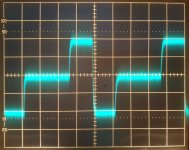
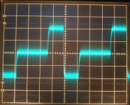
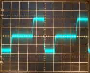
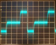
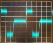
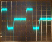
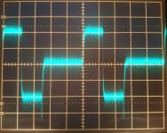
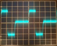
Attached photos from the oscilloscope screen, bit transitions visualized.
0111...1111
1000...0000
1000...0001
0111...1111
1000...0000
1000...0001
Attachments
-
 Bit_0.jpg507.3 KB · Views: 68
 -
 Bit_1.jpg445.3 KB · Views: 56
 -
 Bit_2.jpg492.7 KB · Views: 59
 -
 Bit_3.jpg479.3 KB · Views: 61
 -
 Bit_4.jpg491.4 KB · Views: 58
 -
 Bit_5.jpg506.4 KB · Views: 54
 -
 Bit_6.jpg474.7 KB · Views: 58
 -
 Bit_7.jpg483.1 KB · Views: 68
 -
 Bit_8.jpg474.7 KB · Views: 61
 -
 Bit_9.jpg510.1 KB · Views: 63
 -
 Bit_15_downscaled.jpg495.3 KB · Views: 60
 -
 Bit_15.jpg525.2 KB · Views: 58
 -
 Bit_14.jpg512.7 KB · Views: 66
 -
 Bit_13.jpg489 KB · Views: 66
 -
 Bit_12.jpg487.5 KB · Views: 56
 -
 Bit_11.jpg503.5 KB · Views: 61
 -
 Bit_10.jpg500.4 KB · Views: 60
Note the ugliness of bit #8 and bit #9.
I guess somehow the bit transition "down" is messed up, but why?
And is this one IC (possibly out of normal spec) or architecture specific?
Do you know this:
Nakamichi has a patent on this.
Thor
- Home
- Source & Line
- Digital Line Level
- TDA1541A reducing DNL