I don't see any significant difference between the L and R channel, where the R has a capacitor.
Interesting, I do. There are many harmonics reduced or eliminated. Especially 0dBFS looks a lot cleaner to me.
Thor
It is however the correct thing to do - as previously recommended.. . . I added 4.7 nF between the + and - input of the opamp, it did not make any difference. The glitch amplitude did not change, either.
It defines the signal BW at the input of the I/V amplifier + it reduces the loop-area of the circulating RF current from the DAC output stage.
cheers
PS:
I would recommend to re-locate the cap from the input of the OP, to closer to the analog output of dac chip (right at the output pin).
👍 @lcsaszar
Last edited:
I guess somehow the bit transition "down" is messed up, but why?
And is this one IC (possibly out of normal spec) or architecture specific?
Do you know this:
View attachment 1381020
Nakamichi has a patent on this.
Thor
Seen this Nakamichi patent?
https://patents.google.com/patent/US5034744
It is interesting, but beyond the complexity that I am willing to experiment with. I wonder if it ever went into a commercial product.
Yes, it's trying to eliminate a glitch by injecting a counter glitch. Sounds like a good idea until you try to make it work without adjustment.
Worse, if you get it wrong, you will actually make the glitch worse.
I suspect this patent was not targeted at the TDA1541 which has very limited glitches, but R2R DAC's like PCM53/54/56 etc.
Thor
Magnifying glass
For a low level sinal like this (0.1 mV) it is mandatory to use ground loop avoiding techniques. Also best to power all generator and measuring gear from battery. I power my sound card from an USB battery pack by disconnecting the +5 V (red) wire from the PC and routing it to the battery pack.
I will try the same on the I2S generator, but for now an ADUM3160-based USB isolator seems sufficient.
It is also best to run the laptop with the FFT from the internal battery.
A digital silence should give about 0.5 mV noise (after x100 amplification) on the oscilloscope, without any 50/100 Hz modulation.

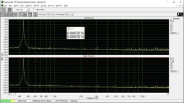
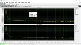


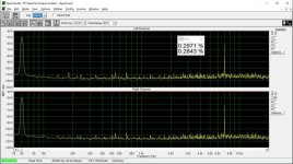


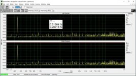
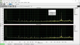

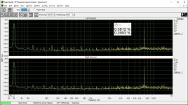
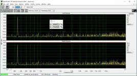
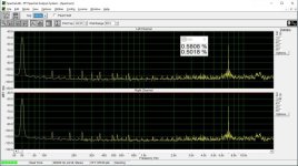
These measurements were done "as is", i.e. no adjustments of the bit error were done.
I must thank you again in advance for your forbearance, but I am at a loss what we are measuring here?
Thor
This is low level harmonic and intermodulation distortion. The signal amplitude is 6 bits peak-to-peak in the digital domain. In addition, there is a digital zero shift by centering the signal around bit #9, bit #10, etc. until bit #15. (Actually bit #15 is analog zero). This shift makes it possible to investigate the magnitude deviation of the bit steps from the LSB, that is their contribution to differential nonlinearity. If the step at e.g. bit #9 is smaller or bigger than the LSB, the DNL at the 0->1 transition at bit #9 is not zero, and this increases low-level distortion.
This way we can test the DNL at the upper 7 bits. It is also possible to improve DNL by injecting some current +/- where we can access the DAC internals through the DEM pins.
This way we can test the DNL at the upper 7 bits. It is also possible to improve DNL by injecting some current +/- where we can access the DAC internals through the DEM pins.
Last edited:
Let's consider bit #9. We have a periodic signal -60 dBFS that is 6 bits in the digital domain. Let's shift it by 0000000111111111. Then in the positive half cycle bit #9 will be always 1, in the negative half cycle always 0. And since the signal in encoded in the lower 6 bits, bit #10 will remain zero. Only bit #9 contributes to DNL (and the lowest 6 bits, but their contribution is constant, whereas that of the "centering" bit is variable).
Same logic if we move the centering to the next bit.
Same logic if we move the centering to the next bit.
- Home
- Source & Line
- Digital Line Level
- TDA1541A reducing DNL