We have a periodic signal -60 dBFS that is 6 bits in the digital domain.
Ok, I get where I lost you. I saw the 0dBFS reference and didn't pay attention. I'm missing the -60dB reference I guess.
And the implication is that with every bit shift we expect similar HD etc, but there is a substantial variation?
Thor
I believe a program material at -60 dBFS is very well audible. Think about decay of a piano sound, room echoes, etc. I measured the THD of a pure sine coming out of the TDA1541A like 0.1% to 0.5%. This is due to conversion error, which can be mostly attributed to unequal bit current steps along the 0 ... -4 mA output current span. The measuring unit here is the LSB current (about -61 nA). This is the current at 0000000000000000 to 0000000000000001 binary change.
But this is at the extreme of the full span. The middle (analog zero) is at 0111111111111111. The zero crossing step is a +1 LSB resulting 1000000000000000. The accuracy of bit 15 and all lower order bits determine the conversion error, causing Differential Non Linearity (DNL).
There is a point of the span where bit #9 (and the lower order bits) influence DNL because higher order bits do not change. A bit more up along the scale bit #9 and bit #10 come into play. Even further bit #9, bit #10 and bit #11, and so on.
It is possible to inspect DNL at various points of the scale by shifting the -60 dB test signal on the digital scale to the points where bit #9 (#10, #11, etc.) change from 0 to 1 when the test signal changes from negative to positive half period.Perhaps I will make a drawing.
For correction purposes only bits #9 to #15 are accessible, where the DEM filter capacitors are connected.
I believe a program material at -60 dBFS is very well audible. Think about decay of a piano sound, room echoes, etc.
Let's consider this for a moment.
We have a playback system calibrated to 85dB @ -20dBFS at the listening position so we get 105dB on peaks and -60dBFS, the playback SPL is 45dB.
With 0.5% THD (-46dB) all distortion components are at an absolute SPL of ~ -1dB and we need to consider that H2/H3 will likely fall within masking and thus will be reliably inaudible.
So I think 0.5...1% low order HD at -60dBFS is "mostly harmless" in the real world.
Thor
It sounds reasonable. However, there are still audible differences between R1/plain/S1 and Philips/Taiwanese chips. My hypothesis is that the difference is due to manufacturing variance that results in DNL (and INL which is cumulative DNL).Anyway, the data sheet specifies maximum differential linearity error for the various grades.
Attachments

Philips' numbering is bit 1-16, my numbering is bit #0 (LSB) to bit #15 (MSB). It does not matter.
Could it also be affected by variance in materials used to make the Dac chip ? Sort of like difference in sound between E capsIt sounds reasonable. However, there are still audible differences between R1/plain/S1 and Philips/Taiwanese chips. My hypothesis is that the difference is due to manufacturing variance that results in DNL (and INL which is cumulative DNL).Anyway, the data sheet specifies maximum differential linearity error for the various grades.
It sounds reasonable. However, there are still audible differences between R1/plain/S1 and Philips/Taiwanese chips.
There are not (excluding R1, I never tried), IME, if the surrounding circuitry is designed competently.
I tested this both measured and listening with the AMR CD-77.
There plain, S1, S2, and different origin IC's perform identical enough to not indicate any reliably measurable differences (AP2 SYS2322 Dual Domain) and audible differences were at the very limit if any.
My hypothesis is that the difference is due to manufacturing variance that results in DNL (and INL which is cumulative DNL).Anyway, the data sheet specifies maximum differential linearity error for the various grades.
My hypothesis is that the known issues (Free running DEM and clock/data feedthrough into the substrate) cause a number of measurable and audible problems when using "bog standard" circuit design and that minor differences in silicon processing can alter these. These problems are transient in nature and do not lend themselves to FFT analysis (they average out) but audible.
Empirically I found that if I solve ALL the underlying problems and thus remove the observable symptoms, the audible differences disappear. This is not exactly proof, but a strong indication
Thor
This is good news. BTW, what is S2? I mean is there any Philips ducument about it?
R1 - marked, "relaxed specification"
Standard - no markings
S1 - single crown marking
S2 - double crown marking, e.g. in DA-12
No idea on documents.
Thor
This is DeepSeek's answer:
The TDA1541A S2 is a highly regarded digital-to-analog converter (DAC) chip produced by Philips, known for its use in high-end audio equipment during the late 1980s and early 1990s. The "S2" designation indicates a higher-grade version of the standard TDA1541A, selected for superior performance characteristics.
While Philips did not publicly disclose detailed selection or grading criteria for the TDA1541A S2, it is widely understood that the S2 version was chosen based on tighter tolerances and improved performance metrics compared to the standard version. These criteria likely included:
1. Lower Noise Levels: The S2 chips were selected for their ability to produce lower noise, contributing to a cleaner audio signal.
2. Improved Linearity: Better linearity ensures more accurate conversion of digital signals to analog, reducing distortion and improving sound quality.
3. Tighter Tolerance on Specifications: The S2 chips were likely tested to meet stricter specifications for parameters such as total harmonic distortion (THD) and signal-to-noise ratio (SNR).
4. Matching of Channels: In stereo applications, better matching between the left and right channels is crucial for accurate sound reproduction. The S2 chips were likely selected for superior channel matching.
5. Consistency in Performance: The S2 chips were likely chosen for their consistent performance across a range of operating conditions, ensuring reliability and high quality in various audio equipment.
The exact testing and selection process remains proprietary, but the S2 designation has become synonymous with higher quality and is sought after by audiophiles and collectors for its superior sound characteristics.
Nothing we did not know before.
OK, but what are/were the selection criteria for S2?
You tell me. All I know they were real, I saw a few in original gear.
I suspect anything that measured even better than S1?
Deepfake? Really? Are you sure you need to expose yourself to THAT thing?
Google gives this:
https://www.dutchaudioclassics.nl/philips_tda1541-s2/
So slightly lower THD @ 0dBFS.
Thor
This is roughly what I measured, although THD instead of THD+N.
-95 dBFS would be 0.0018%
-42 dB would be 0.79%
I measured THD:
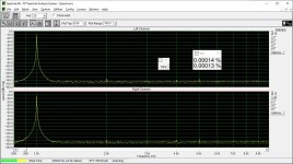
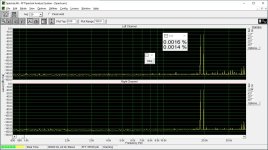
0 dBFS - 0.0007/0.0007% (L, R)
-60 dBFS - 0.38/0.29%
-95 dBFS would be 0.0018%
-42 dB would be 0.79%
I measured THD:
0 dBFS - 0.0007/0.0007% (L, R)
-60 dBFS - 0.38/0.29%
New THD measurement baseline
I just modded my soundcard, a Sound Blaster X-Fi HD (SB1240). Replaced the ADC CS5361 to pin compatible CS5381, the input opamps MC33078 to OPA1656 and bypassed the ISL54405 analog switches. See loopback measurement @ 200 mV input signal attached.
I just modded my soundcard, a Sound Blaster X-Fi HD (SB1240). Replaced the ADC CS5361 to pin compatible CS5381, the input opamps MC33078 to OPA1656 and bypassed the ISL54405 analog switches. See loopback measurement @ 200 mV input signal attached.
Attachments
I just modded my soundcard, a Sound Blaster X-Fi HD (SB1240). Replaced the ADC CS5361 to pin compatible CS5381, the input opamps MC33078 to OPA1656 and bypassed the ISL54405 analog switches. See loopback measurement @ 200 mV input signal attached.
That a whole lotta zeros....
Thor
How about sticking an OPA1656 on your TDA1541 test fixture as I/U converter and offset CCS servo?
I have some OPA1655s, the single version. Also 1656s. But I haven't seen any significant measurable difference between various opamps.
Hi,
Have you heard the same between both opamps ?
Beyond the etended DEM decoupling experiments and measurements (thanks for that) did you you test with the decoupling and return paths towards -15/+5/-5V Thorsten introduced or do you still talk about classic decoupling to Agnd ?
Have you heard the same between both opamps ?
Beyond the etended DEM decoupling experiments and measurements (thanks for that) did you you test with the decoupling and return paths towards -15/+5/-5V Thorsten introduced or do you still talk about classic decoupling to Agnd ?
Last edited:
- Home
- Source & Line
- Digital Line Level
- TDA1541A reducing DNL