It is possible to reduce the DNL of the upper 6 or 4 bits. I am not sure what else is the difference between the various grades. The data sheet has not much information.
Here is an article from Pedja about the TDA1541A grading and differences between the production runs. His measurements at -60 dBFS are consistent with mine.
https://www.audialonline.com/blog/tda1541a-and-model-s-usb-part-4-tda1541a-grades-and-series/
https://www.audialonline.com/blog/tda1541a-and-model-s-usb-part-4-tda1541a-grades-and-series/
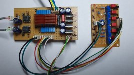
Hi you've gotten me very curious about this circuit. Kudos. I've been playing & tweaking my AyA for years.Compensation circuit diagram.
Its on S1 chip & wondering if further improvement can be had. So your saying to apply null only at these 8 pins
with a -15v supply. What about the bypass caps, does it stay or removed. Thanks again for sharing. Btw I've tested
KZ 100uf 25v made improvement but sound was too much in your face but when I changed to KZ 100uf 50v yes
found magic. Tried KL sometime back just didn't like what I heard so gave up the thought until I saw your thread &
it got me curious to give it another go cause I know the sound of KZ well. Cheers & thanks again for sharing
What about the bypass caps, does it stay or removed.
The compensation circuit is an add-on. The 10M resistors go directly to the DEM filter pins, the capacitors will remain as they are.
The compensation circuit is an add-on. The 10M resistors go directly to the DEM filter pins, the capacitors will remain as they are.

Many thanksWhat about the bypass caps, does it stay or removed.
The compensation circuit is an add-on. The 10M resistors go directly to the DEM filter pins, the capacitors will remain as they are.
Sorry I dont, in terms of SQ it is immediately obvious but after burn in, leaps even further.@sumotan, Do you have FFT measurements of the KZ setup it will be interresting to see how they behave in real life
.
you just have to try it
After any change in my setup I normaly make measurements before listennig session to avoid bias of any kind
good measurements are not straight to great sound , but great sound never comes from bad measurements 😉
the UKZ 100 uf / 50 v are to big for my board , but if I will try I will post measurements for you all 🙂
.
good measurements are not straight to great sound , but great sound never comes from bad measurements 😉
the UKZ 100 uf / 50 v are to big for my board , but if I will try I will post measurements for you all 🙂
.
Last edited:
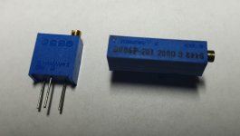
If you want to compensate all 6 bits, here is the full diagram. X1 to X6 are removable jumpers.
It's a very cool idea you have here , but the cost is prohibitive , I wish I could 🙂
.
Why would it be cost prohibitive Fabrice. It's just trim ports & resistors.
Does not cost much to fabricate a -15v supply as it's a low current supply.
main issue is how to execute the connections as to many long wires might
turn in an antenna for picking up RF etc I think.
Does not cost much to fabricate a -15v supply as it's a low current supply.
main issue is how to execute the connections as to many long wires might
turn in an antenna for picking up RF etc I think.
I can assure you it is not sensitive to EMF pickup. One side of the 10M resistor goes to a relatively low impedance point, the wiper of the trimmer. The other side with the long wire goes to the decoupling capacitor, which is again shunting any RF and mains pickup.Why would it be cost prohibitive Fabrice. It's just trim ports & resistors.
Does not cost much to fabricate a -15v supply as it's a low current supply.
main issue is how to execute the connections as to many long wires might
turn in an antenna for picking up RF etc I think.
The -15V is available at pin 15.
I haven't found any stability issue with Bourns 3296, the horizontal type should be good, too.
https://www.bourns.com/pdfs/3296.pdf
Attachments

Very nice so tapping into the -15 supply would not hurt SQ ? Wow be great though if a comparison between Stock vs S1 can be conducted. On my dac stock chip aside frm being slightly rough on terrible, the layering is not as good & sound stage push forward as compared to S1
Cheers & thanks again
Cheers & thanks again
In the AMR CD 77 he uses just two polymer cap for the two first DEM a little far from the pins saying inductance was not as much critical here.
Nope, not what I did, I used a Film cap same as the other DEEM Pin's plus Os-Con's.
The Film Cap's have their minimum impedance at several MHz and the Os-Con around 200kHz.
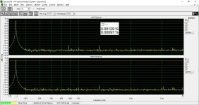
There was a warmup period, after that distortion was stable and low.
But who knows, Rogic as Loesch say the ultra low noise thingy is not the first item on their list when they designed DAC with this chip...
And here is why:
-15V still has around 60dB ripple rejection.
So 1mV noise between AGND & -15V translates into around 1uV output noise re 2V or -126dB.
So we want quiet supplies but no need to to chase 1nV|/Hz.
Thor
Off topic, but still about digital currents:
About digital spread current inside the digital section towards the analog one (and so the output) inside the chip that certainly asked a AGND and DGND pin to be tied outside in order to reduce a little that stray capacitance.
And as the number of layers are less expensive nowadays, could it work to make further appart the meeting point of the two pins, not only in order to avoid close chip else currents near pins contamination, but also to reduce stray capacitance or cross talkings ?
Two plain reference layers in spite of one; one for each of the two ground ic pins ; but tied together aways, very close to the common point of the layers near the PS ? the stray capacitance between the two pins is about the gap between them, so better maybe the bigger gap is the horizontal one between AGND pin and DGND pin, and so need perhaps of two layers that meet (I mean the vertical gap between both is at max in the 1.6 mm pcb thickness limit related how you space both layers) ?
We want a quiet reference between both pins and the nearest low Z between both as well ! we could also just tie them 3D with a wire in serie till th star ground meeting point ?
I try to think not just to measure. Btw the measurement before the listening can of course biass you so the listening if you think serioussly. No toys to show, nore big screens. Understanding before measuring seems important to me as the quality of the measurement tools (probe, scope...) AND even more to understand the threshold of numbers vis à vis of the particular chip with what the ears can hear related ! There is no doubt for me the eyes can biass the ears.
So thanks again T. I understand a little more with the post above. Indeed Pedja is using even no V regs but "quiet stabilizers" with low impedance output, zener that feed a jfet to its max in order that last has the lowest noise : simple effective and strangly even better when not post decoupled if already very near from the TDA1541A (just few nano only at the pin 15, it seems he liked that simplified decoupling I made since the AYA 2014; certainly noiser, but the noiser added by thhe lack of the last near pin lythic decoupling should be lower than the threshold you talk about. It becomes more lively on the sound side, even more if you just decouple the -15V only.... very surprising ! Of course will noy work in the context of your newest layout ! )
cheers, no measurement or toys to show, just a drink here (but ask Pedja that measured that) or it is on the blog (AYA 2 to AYA4 and its manuals) .
Attachments


Last edited:
BTW


Just story to show something big !
In the UKZ 100 uF value: The 25V has the lowest leakage. The 100V the least ESR but that is of a less importance here for the 14 DEMs.
Just story to show something big !
In the UKZ 100 uF value: The 25V has the lowest leakage. The 100V the least ESR but that is of a less importance here for the 14 DEMs.
Yes I noticed too but please be careful: the leakage current of a capacitor is defined as the current flowing while Rated Voltage is applied accross the terminals.
In the same time, we know that leakage current increase with applied voltage!
So the difference You perceive in the datasheet is that the higher voltage units are tested at... higher (rated) voltages!
I bet the reality is instead that at the same test voltage the higher rated caps would show nicely less leakage current..
Ciao, George
Inductance, won by the 25V/50V VS the 100V (for UKZ for whom who like it) due to the non usual bigger space pin of the 100V at Nichicon.
UKLs have of course very low leakage but even lowest inductance choice. I surmise we have to choose the UKL 16V cause in 10V the first value is 150 uF. A pity we have not more value choice at 10V (DEM is 7V around with normal conf, then T. gave the V values with its screen cap by cap DEM pin.
Edit : Hey George, thanks, I believed you was in holyday, had you have time to populate ? (PM)
- Home
- Source & Line
- Digital Line Level
- TDA1541A reducing DNL