A diagram might help!
A bridge driving circuit was posted here 4 x BTL 300W/8R - a TDA8950j based 4 channel power amplifier - diyAudio towards the end of the thread. or there are a few circuits on Rod Elliott's site. Here is one Bridging Adapter For Power Amps
... and here in this thread too ... 😉
http://www.diyaudio.com/forums/class-d/255046-systemd-liteamp.html#post4225966
There you can find some hints for bridge mode tuning to get best THD+N.
Note: in bridging mode the distortions are a little bit higher as running each amplifier isolated.
Don't forget: Markus (exceptional good!) LiteAmp inverts the input signal! So if you drive the LiteAmp with your own or with my "bridge gain pre-amplifier" then don't forget to swap the inputs!
BR, Toni
Toni thank you for the information.
When you say that Markus's LiteAmp swaps the input do you mean that the amplifier is inverting?
I see your bridge adaptor is inverting and looks to have a gain of approx 4. My preamp output is 10v into 15k. So I think I can drive the bridged amps without adding the gain board if I use your bridge adaptor?
Toni thank you for the information.
When you say that Markus's LiteAmp swaps the input do you mean that the amplifier is inverting?
I see your bridge adaptor is inverting and looks to have a gain of approx 4. My preamp output is 10v into 15k. So I think I can drive the bridged amps without adding the gain board if I use your bridge adaptor?
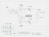
If your preamp has too high output impedance but enough gain you can use this simple single ended to balanced circuit (gain = 1x) connected directly to LiteAmp mainboard. Maybe you need to reduce C2 (RF filter resumes your preamp is able to drive 600R).
BR, Toni
Attachments
Two options.
If you want to bridge it without gain boards you can use the bridging circuit from astx or any circuit with equivalent function.
If you use the gain boards you do not need anything else.
The fully symmetrical inputs allow wiring for inverting, non inverting and bridged operation.
Here a wiring diagram for bridged operation:
https://en.wikipedia.org/wiki/Bridged_and_paralleled_amplifiers
Note: The LiteAmp is well suited for bridged operation, but not for parallel operation.
Note: If you dislike the complexity of the gain board - you can skip the limiter, which makes half of the gainboard.
Last edited:
ChocoHolic, I have a few ideas at the moment as to how I will use the Liteamp and what speakers I will use. If I need a bit more gain, can I increase R7? I assume the gain is set by R7/(R10+R12) realise that this would increase the noise but I may be able to accept slightly more noise.
Is there anything else I should consider before attempting to change the gain?
Is there anything else I should consider before attempting to change the gain?
Changing R7 will directly hit into loop gain, step response, oscillation frequency...
It is better to reduce R10+R12 and proportionally increase C4.
It is better to reduce R10+R12 and proportionally increase C4.
I guess I shall build with stock gain of 4.9 then as I do not want to lower the input impedance too much especially as I believe the Pre Amp will have enough output to drive the amplifiers.Changing R7 will directly hit into loop gain, step response, oscillation frequency...
It is better to reduce R10+R12 and proportionally increase C4.
55V Update, Correction
By chance I noticed a silly error in the untested 55V BOM.
Keeping D3 unchanged with a 100V rating is obviously wrong.
D3 shall have at least a 150V rating (more common will be 200V).
It can be either a 150V shottky or simply two of the MBR1100 in series.
Alternatively an ultrafast diode with soft recovery and trr=50ns (30ns preferrable) or less should work as well.
Hope this correction comes in time or had been noticed by potential 55V-enthusiasts.
It would be unnecessary to fail just because of such inadvertence.
Again, please everybody be aware that the 55V-version is untested and intended as a starting point for DIYers with R&D skills.
Attached the updated 55V-BOM.
By chance I noticed a silly error in the untested 55V BOM.
Keeping D3 unchanged with a 100V rating is obviously wrong.
D3 shall have at least a 150V rating (more common will be 200V).
It can be either a 150V shottky or simply two of the MBR1100 in series.
Alternatively an ultrafast diode with soft recovery and trr=50ns (30ns preferrable) or less should work as well.
Hope this correction comes in time or had been noticed by potential 55V-enthusiasts.
It would be unnecessary to fail just because of such
inadvertence.Again, please everybody be aware that the 55V-version is untested and intended as a starting point for DIYers with R&D skills.
Attached the updated 55V-BOM.
Attachments
By chance I noticed a silly error in the untested 55V BOM.
Keeping D3 unchanged with a 100V rating is obviously wrong.
D3 shall have at least a 150V rating (more common will be 200V).
It can be either a 150V shottky or simply two of the MBR1100 in series.
Alternatively an ultrafast diode with soft recovery and trr=50ns (30ns preferrable) or less should work as well.
Hope this correction comes in time or had been noticed by potential 55V-enthusiasts.
It would be unnecessary to fail just because of such
Again, please everybody be aware that the 55V-version is untested and intended as a starting point for DIYers with R&D skills.
Attached the updated 55V-BOM.
I dont think anyone has started doing the R&D for this one, I would... but I dont have a +/-55 supply at hand.

With that said with a higher voltage, is it correct in assuming the loop response remains unchanged ? How does one even R&D test with modications made? Play continuous loud music for hours and observe performance? as well as momentary shorting the output stage at high output levels..
I think it would be obvious to have mandatory protection schemes like fusing and DC offset sense at the speaker output.
Last edited:
A class D amplifier's loop gain varies with supply voltage. Bruno's papers "Simple Self-Oscillating Class D Amplifier with Full Output Filter Control" and "Globally Modulated Self-Oscillating Amplifier with Improved Linearity" available for download from Hypex are good starting points.
Dependency of the loop gain from supply rails:
Obviously the magnitude of the comparator output is proportionally growing with the rails.
But at the same time also the triangle carrier grows in the same manner.
In equation (4) of Brunos "Simple Self-Oscillating Class D Amplifier with Full Output Filter Control"
you see that both effects fully cancel out.
Also in reality loop gain is stable over a wide range of the rail levels.
Despite the lite amp having different additional transfer functions involved,
the independency of the loop gain from the rail voltage applies in the same manner.
Step response of the complete amp:
In order to reach clipping with same input level, I increased the closed loop voltage gain of the amp,
by reducing the input resistors. There I also increased the low pass cap.
Increase of the chosen low pass cap is slightly more than the reduction of the resistors.
==> Step response is slightly slower, but of perfect shape.
Testing:
High power long term music and short circuiting at high signals are more the things you can do,
after you have finished the R&D work and when you are convinced that it is bullet proof.
Before that - better go through the points below.
Please understand that this is not a full R&D manual, but just a rough overview.
Whenever you observe behaviors, which do not fit to your theoretic expectation or design goals,
then search the error, which can be in the proto and/or your theory.
Every point where you are not able to bring both to identical 'opinions', increases your risk to fail,
but fortunately few open questions do not immediately make success impossible.
Testing / R&D work to be done for 55V:
- Double check if the values in the BOM are making sense from theory:
SIM: Adjust simulation to the new values and see if fs, step response, stability etc fit.
stone age hand calculations: Check if biasing components auxiliary supplies etc. and IR + MosFet specific values including parametrization of dead time and over current do fit.
- Based on the theoretic expectations from above and after setting up the proto check/correct things as below:
In the beginning work with current limited supply (0.5A limitation is a good choice here)
Aux supplies
DC operating points
Basic oscillation
Timings of the gate drive in idle situation
Signal shapes and signal integrity in the small signal area
After all this is fine you can go for a stronger supply:
-Examine switching wave shapes as described below, but stay with load currents around 4A.
-Check the overcurrent protection by using a 50uH+0.1R load and small input signal (anything between 100Hz...1kHz) slowly increasing until
you reach the shut down. If shut down still does not happen at 10% above the desired level - stop and readjust!
Test high side limits independend from low side limits, simply by disabling always the opposite protection.
-After this, recheck switching wave shapes 3) 4) 5) 6) with currents close to shut down.
Examination of switching wave shapes:
Amp without input signal (input shorted).
1) Idle/no load, event of turning off the low side MosFet
2) Idle/no load, event of turning on the low side MosFet
3) Sink load current. Resistor from pos rail to amp output, event of turning off the low side switch.
4) Sink load current. Resistor from pos rail to amp output, event of turning on the low side switch.
5) Source load current. Resistor from neg rail to amp output, event of turning off the low side switch.
6) Source load current. Resistor from neg rail to amp output, event of turning on the low side switch.
Typically, I do not have the load towards the rail connected when staring up the amp, but connect it manual just for the short time of doing the measurement. Easy for the LiteAmp, but for the 2kW monster and involved currents and voltages this game always was an impressive welding event at the contact point.... Better wear glasses.
Alternatively you could use some proper electronic relay, but the arcing during the manual test can also be seen as a ruggedness test.
For measurements 3,4,5,6 start with reasonably small currents, because untamed and badly ringing half bridges will burn at higher currents.
Interesting current levels start when the load current is larger than the filter ripple current.
So measure - adjust - measure - adjust- measure - increase load - measure - ....
If you use an isolated floating power supply, then all this can be done even without the need of differential probes.
Do not try to simulate equivalent situations by applying DC to the amp input with load from amp output to GND. DC signal and load to GND would cause heavy bus pumping!
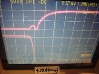
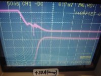
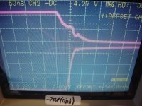
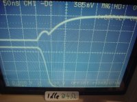
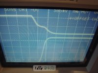
All attached screen shots were taken with the following settings:
Time scale is 50ns per horizontal grid.
Upper trace: Ugs of the low side switch, 5V per vertical grid
Lower trace: Half bridge output voltage, 20V per vertical grid
Obviously the magnitude of the comparator output is proportionally growing with the rails.
But at the same time also the triangle carrier grows in the same manner.
In equation (4) of Brunos "Simple Self-Oscillating Class D Amplifier with Full Output Filter Control"
you see that both effects fully cancel out.
Also in reality loop gain is stable over a wide range of the rail levels.
Despite the lite amp having different additional transfer functions involved,
the independency of the loop gain from the rail voltage applies in the same manner.
Step response of the complete amp:
In order to reach clipping with same input level, I increased the closed loop voltage gain of the amp,
by reducing the input resistors. There I also increased the low pass cap.
Increase of the chosen low pass cap is slightly more than the reduction of the resistors.
==> Step response is slightly slower, but of perfect shape.
Testing:
High power long term music and short circuiting at high signals are more the things you can do,
after you have finished the R&D work and when you are convinced that it is bullet proof.
Before that - better go through the points below.
Please understand that this is not a full R&D manual, but just a rough overview.
Whenever you observe behaviors, which do not fit to your theoretic expectation or design goals,
then search the error, which can be in the proto and/or your theory.
Every point where you are not able to bring both to identical 'opinions', increases your risk to fail,
but fortunately few open questions do not immediately make success impossible.
Testing / R&D work to be done for 55V:
- Double check if the values in the BOM are making sense from theory:
SIM: Adjust simulation to the new values and see if fs, step response, stability etc fit.
stone age hand calculations: Check if biasing components auxiliary supplies etc. and IR + MosFet specific values including parametrization of dead time and over current do fit.
- Based on the theoretic expectations from above and after setting up the proto check/correct things as below:
In the beginning work with current limited supply (0.5A limitation is a good choice here)
Aux supplies
DC operating points
Basic oscillation
Timings of the gate drive in idle situation
Signal shapes and signal integrity in the small signal area
After all this is fine you can go for a stronger supply:
-Examine switching wave shapes as described below, but stay with load currents around 4A.
-Check the overcurrent protection by using a 50uH+0.1R load and small input signal (anything between 100Hz...1kHz) slowly increasing until
you reach the shut down. If shut down still does not happen at 10% above the desired level - stop and readjust!
Test high side limits independend from low side limits, simply by disabling always the opposite protection.
-After this, recheck switching wave shapes 3) 4) 5) 6) with currents close to shut down.
Examination of switching wave shapes:
Amp without input signal (input shorted).
1) Idle/no load, event of turning off the low side MosFet
2) Idle/no load, event of turning on the low side MosFet
3) Sink load current. Resistor from pos rail to amp output, event of turning off the low side switch.
4) Sink load current. Resistor from pos rail to amp output, event of turning on the low side switch.
5) Source load current. Resistor from neg rail to amp output, event of turning off the low side switch.
6) Source load current. Resistor from neg rail to amp output, event of turning on the low side switch.
Typically, I do not have the load towards the rail connected when staring up the amp, but connect it manual just for the short time of doing the measurement. Easy for the LiteAmp, but for the 2kW monster and involved currents and voltages this game always was an impressive welding event at the contact point.... Better wear glasses.
Alternatively you could use some proper electronic relay, but the arcing during the manual test can also be seen as a ruggedness test.
For measurements 3,4,5,6 start with reasonably small currents, because untamed and badly ringing half bridges will burn at higher currents.
Interesting current levels start when the load current is larger than the filter ripple current.
So measure - adjust - measure - adjust- measure - increase load - measure - ....
If you use an isolated floating power supply, then all this can be done even without the need of differential probes.
Do not try to simulate equivalent situations by applying DC to the amp input with load from amp output to GND. DC signal and load to GND would cause heavy bus pumping!
All attached screen shots were taken with the following settings:
Time scale is 50ns per horizontal grid.
Upper trace: Ugs of the low side switch, 5V per vertical grid
Lower trace: Half bridge output voltage, 20V per vertical grid
Attachments
Due to closed loop gain tracking the rails to take advantage of the available power, yep. I should have been specific to say that, with adjustment to also maintain switching frequency, differences are necessarily small.Also in reality loop gain is stable over a wide range of the rail levels.
Interesting data; thank you for sharing. What is the scope+probe bandwidth?All attached screen shots
Interesting data; thank you for sharing. What is the scope+probe bandwidth?
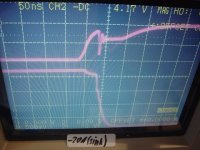
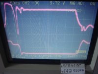
This very smooth and soft approaching of the Vds at the rails is something special of the IRFI4212. With most Fets you will find Vds hitting to the rail more hard.
For reference I am attaching a measurement with a halfbridge based on IRFB4115 when sinking 41A.
Upper trace is Vgs of the low side Mos, 5V/Div
Lower trace is Vds of the low side Mos, 50V/Div
The 25V step in Vds in the first grid is mostly the inductive voltage drop of the rails + upper MosFet package while the lower MosFet first takes over the load current and then removes Qrr. Together this takes 50ns with an di/dt of approx 2000A/us.
The deep dip in Vgs happens when Qrr is removed and Crss feeds the giant dv/dt from the Vds to the gate - superimposed with an inductive effect of the giant di/dt in the source wire when the Qrr-removal-current-peak snaps back.
Both half bridges (IRFI4212 in the LiteAmp & IRFB4115 in the SystemD_MD) have proper snubbers in place. Otherwise heavy ringing would happen, when driven with such speed and current levels.
Scope is the good old 500MHz analogue Iwatsu TS-8500 (...yes John, I am still using it. 😎 )
Probes are the ELDITEST GE4512 (Bandwidth: 450MHz)
Attachments
Last edited:
Dependency of the loop gain from supply rails:
Obviously the magnitude of the comparator output is proportionally growing with the rails.
But at the same time also the triangle carrier grows in the same manner.
In equation (4) of Brunos "Simple Self-Oscillating Class D Amplifier with Full Output Filter Control"
you see that both effects fully cancel out.
Also in reality loop gain is stable over a wide range of the rail levels.
Despite the lite amp having different additional transfer functions involved,
the independency of the loop gain from the rail voltage applies in the same manner.
Thank you very much for the detailed explanation I really appreciate the effort.
Ive look at equation 4. ive also looked at hysteresis switching waveform with output voltage increase vs fs.I am still looking at the "additional transfer functions involved" from the simulation files.
I will take your R&D advice as an unofficial guide to upgrading, those wave shots at idle, -Ids, +Ids looks squeaky clean 😀
Lower trace: Half bridge output voltage, 20V per vertical grid
Note: Half bridge output voltage measured vs neg rail. Means Vds, directly at the MosFet.
Hi
Anyone can recommend me an equivalent for Q1: 2SC5171 that is available at Mouser?
Thank you!
Anyone can recommend me an equivalent for Q1: 2SC5171 that is available at Mouser?
Thank you!
Ups... and for U101, U103 the same from the gain board. I will place today the order to Mouser so I want to include as many parts as I can in one order.
Thank you!
Thank you!
- Home
- Amplifiers
- Class D
- SystemD LiteAmp