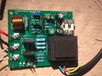
Finished SSR PCB
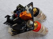
Just finished and tested my SSR.
SSR is based on the TA7317 chip which operates 2 VOM1271 photovoltaic drivers which outputs are parallelled to drive 2 IRFP4568 FET's.
Measured DC resistance is 14.5mOhm. This is measured with currents in a range from 10ma to 3A. DC resistance doesn't change. (Measured with fluke 8808)
Turn off thump is not existing, turn on delay can trimmed to about 10seconds maximum.
DC detection is according graph a couple posts back.
This PCB is getting the mains supply from the soft start PCB.
Forgot the pictures
It is never a good idea to route input/output in transformer proximity.
Why exactly?
Picking up noise, safety reasons?
PCB tracks for signal are as short as possible, but the output air coil can pick up noise... yes, I think I can follow you. I'll keep it in mind for the next revisions of my SSR PCB.
Thanks
Picking up noise, safety reasons?
PCB tracks for signal are as short as possible, but the output air coil can pick up noise... yes, I think I can follow you. I'll keep it in mind for the next revisions of my SSR PCB.
Thanks
Nice work!
Can you share the pcb?
Regards.
Offcourse,
Gerber files is the .zip file.
Regards
Attachments
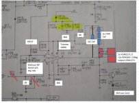
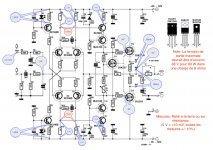
I have designed 3 generations of speaker protect circuit.
The left one is a mechanical relay with dc detect and power up delay.
The middle one is solid state relay with dc detect and power up delay.
The right one is solid state relay with dc detect, over current detect and power up/down detect. All three use a PIC micro to get some intelligence into them.
The left one is a mechanical relay with dc detect and power up delay.
The middle one is solid state relay with dc detect and power up delay.
The right one is solid state relay with dc detect, over current detect and power up/down detect. All three use a PIC micro to get some intelligence into them.
An externally hosted image should be here but it was not working when we last tested it.
I have designed 3 generations of speaker protect circuit.
The left one is a mechanical relay with dc detect and power up delay.
The middle one is solid state relay with dc detect and power up delay.
The right one is solid state relay with dc detect, over current detect and power up/down detect. All three use a PIC micro to get some intelligence into them.
An externally hosted image should be here but it was not working when we last tested it.
Could you share schematic and code (source code and hex) from the biggest board (the one with over current), please?
We all in forum thank you to provide us your expertise.
Ronaldo
Code below picture.Could you share schematic and code (source code and hex) from the biggest board (the one with over current), please?
We all in forum thank you to provide us your expertise.
Ronaldo

;INTH0.ASM
;**********
;INTERNAL OSC, INTERNAL MCLR, POWER UP TIMER ON
LIST R=DEC
LIST P=PIC12F509
;INCLUDE REGISTER DEFINITIONS
INCLUDE P12F509.INC
;_MCLRE_ON EQU H'0FFF'
;_MCLRE_OFF EQU H'0FEF'
;_CP_ON EQU H'0FF7'
;_CP_OFF EQU H'0FFF'
;_WDT_ON EQU H'0FFF'
;_WDT_OFF EQU H'0FFB'
;_LP_OSC EQU H'0FFC'
;_XT_OSC EQU H'0FFD'
;_IntRC_OSC EQU H'0FFE'
;_ExtRC_OSC EQU H'0FFF'
__CONFIG _MCLRE_OFF & _WDT_OFF & _CP_OFF & _IntRC_OSC
INCLUDE MACRO.ASM
;ACCESSES REGISTER BANK BIT
#DEFINE RB0 STATUS,5
;
#DEFINE RL1 GPIO,5 ;SPEAKER SSR RELAY
#DEFINE POSITIVE GPIO,0 ;POSITIVE GOING I/P
#DEFINE NEGATIVE GPIO,1 ;NEGATIVE GOING I/P
#DEFINE MAINS GPIO,4 ;MAINS DETECT
#DEFINE OCMINUS GPIO,2 ;overload negative going audio
#DEFINE OCPLUS GPIO,3 ;overload positive going audio
STATEA EQU 0X1F
FIRSTA EQU 0
FIRSTB EQU 0
;***********************
FIRSTRAM EQU 7 ;JUST POINTER TO FIRST RAM LOCATION
DEL1 EQU 7
DEL2 EQU 8
DEL3 EQU 9
COUNT EQU 10
;COUNTH EQU 11
MAINSCOUNT EQU 12
;MAINSCOUNTH EQU 13
LASTTIMER EQU 14
FLAGS EQU 15
#DEFINE MAINS_TIMERFLAG FLAGS,0
#DEFINE DC_TIMERFLAG FLAGS,1
LASTRAM EQU 1FH
;;;;;;;;;;;;;;;;;;;;;
ORG 0
movwf OSCCAL
RESTART MOVLW FIRSTA
MOVWF GPIO
MOVLW STATEA
TRIS GPIO
;SET UP TIMER AS MIGHT HAVE BROWNED OUT
CLRWDT
MOVLW 0C7H ;SET UP TIMER0 FOR 1.024 MS CHANGE FERQUENCY.
OPTION
CLRF FLAGS
CLRF LASTTIMER
;POWER UP DELAY
;ALLOW AMP TO SETTLE FOR 4 SECONDS
CALL WAIT1SEC
CALL WAIT1SEC
CALL WAIT1SEC
CALL WAIT1SEC
CALL RESETMAINSCOUNT
;;;;;;;;;;;;;;;;;;;;;;;;;;;;;;;;;;;;;;;;;;;;;;;
MLOOP BSF RL1
BTFSC POSITIVE
GOTO POSGOING
BTFSS NEGATIVE
GOTO NEGGOING
CALL TIMERUPDATE
CALL DOMAINS ;SEE IF MAINS GONE
ANDLW 255
BNZ RESTART
BTFSC OCPLUS ;GO IF OVER CURRENT
GOTO BROKE1
BTFSC OCMINUS ;GO IF OVER CURRENT
GOTO BROKE1
GOTO MLOOP
;DONT ALLOW POSITIVE TO KEEP GOING FOR MORE THAN 200MS
POSGOING
MOVLW LOW 200 ;200MS
MOVWF COUNT
PLOOP BTFSC OCPLUS ;2
GOTO BROKE1
BTFSC OCMINUS ;2
GOTO BROKE1
CALL TIMERUPDATE
CALL DOMAINS
ANDLW 255
BNZ RESTART ;go if mains went and came back
BTFSS POSITIVE ;2
GOTO MLOOP ;POS GONE SO OK
BTFSS DC_TIMERFLAG
GOTO PLOOP
BCF DC_TIMERFLAG
DECF COUNT,F
BNZ PLOOP
GOTO BROKE1
BROKE1
BCF RL1
GOTO BROKE1
;;;;;;;;;;;;;;;;;;;;;;;;;;;;;;;;;;;;;;;;;;;;;;;;;;;;;;;
;DONT ALLOW NEGaTIVE TO KEEP GOING FOR MORE THAN 200MS
NEGGOING MOVLW 200 ;200MS
MOVWF COUNT
NLOOP BTFSC OCPLUS
GOTO BROKE1
BTFSC OCMINUS
GOTO BROKE1
CALL TIMERUPDATE
CALL DOMAINS ;SEE IF MAINS GONE
ANDLW 255
BNZ RESTART ;go if mains went and came back
BTFSC NEGATIVE
GOTO MLOOP ;NEG GONE SO OK
BTFSS DC_TIMERFLAG
GOTO NLOOP
BCF DC_TIMERFLAG
DECF COUNT,F
BNZ NLOOP
GOTO BROKE1
;************************
WAIT1MS MOVLW 1
GOTO MSS
MS250 MOVLW 250
MSS MOVWF DEL1
MS MOVLW 249
MOVWF DEL2
DD CLRWDT
DECFSZ DEL2,F
GOTO DD
DECFSZ DEL1,F
GOTO MS
RETLW 0
;***********************
WAIT1SEC
CALL MS250
CALL MS250
CALL MS250
GOTO MS250
;*************************
TEST
BSF RB0
MOVLW 0
MOVWF GPIO
BCF RB0
TEST1
CLRWDT
MOVLW 0
MOVWF GPIO
MOVLW 255
MOVWF GPIO
GOTO TEST1
;*******************************
;CHECK IF MAINS PHASE CHANGED IN TIME
DOMAINS MOVF GPIO,W ;if 1 then mains there
ANDLW 16
BZ NOTCHANGED
;MAINS THERE SO RESET COUNTER
GOTO RESETMAINSCOUNT ;RET VIA
NOTCHANGED
BTFSS MAINS_TIMERFLAG
RETLW 0
BCF MAINS_TIMERFLAG
INCF MAINSCOUNT,F
MOVLW 20
XORWF MAINSCOUNT,W ;20MS
BZ BROKEMAINS
CARRYON RETLW 0;
;IF MAINS COMES BACK RESTART
BROKEMAINS BCF RL1
CALL RESETMAINSCOUNT
BM2 MOVF GPIO,W
ANDLW 16
BZ BM2
;MAINS COME BACK SO RESTART PIC
RETLW 1 ;ERROR
;*****************************************
RESETMAINSCOUNT CLRF MAINSCOUNT
RETLW 0
;******************************************
TIMERUPDATE
MOVF TMR0,W
ANDLW 4
XORWF LASTTIMER,W
BNZ CHANGED
RETLW 0
CHANGED MOVF TMR0,W
ANDLW 4
MOVWF LASTTIMER
BSF MAINS_TIMERFLAG
BSF DC_TIMERFLAG
RETLW 0
;**************************
END
LKA, great project! Thank you for sharing it here.
If I'm not using dual-mono PS, just on PS for both channels, do I have to do any changes?
If I'm not using dual-mono PS, just on PS for both channels, do I have to do any changes?
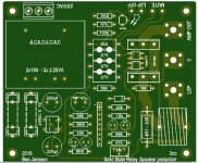
the finalized SSR2 protection
View attachment 765166
View attachment 765167
View attachment 765168
schematic and gerbers
SSR - Google Drive
LKA, great project! Thank you for sharing it here.
If I'm not using dual-mono PS, just on PS for both channels, do I have to do any changes?
thanks, no changes are needed
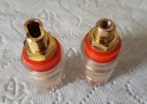
One possible mounting of my SSSR protection board.
1/ get similar binding posts like these 2Pcs Amplifier Speaker Cable Terminal Binding Post 4mm Banana Socket Connector 826962552100 | eBay
2/ cut and align
3/ make M5 internal thread
4/ use non-magnetic bolts and washers
1/ get similar binding posts like these 2Pcs Amplifier Speaker Cable Terminal Binding Post 4mm Banana Socket Connector 826962552100 | eBay
2/ cut and align
3/ make M5 internal thread
4/ use non-magnetic bolts and washers
Attachments


LKA, thanks you for sharing..Great protection
Will use the SSR with a 12V Aux PSU
Can you give us some guidance on how to select D8 TVS bipolar? too many and confused..Thanks
FR
Hi,
(Mosfet Vds) > (2x PSU_V+)
(PSU_V+) < (TVS Vr) < (TVS Vc) < (Mosfet Vds)
So, for 120V mosfet (max +-55V PSU at idle) use
P6KE68CA,P6KE75CA - TH, pcb front side
P6KE75CA Littelfuse | Mouser Europe
or
SM15T68CA - SMD, pcb back side
SM15T68CA STMicroelectronics | Mouser Europe
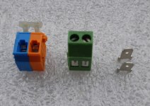
X1 terminal options
WAGO255
https://uk.farnell.com/wago/255-401/terminal-block-wire-to-brd-1pos/dp/4015319
SCREW
https://eu.mouser.com/ProductDetail...=sGAEpiMZZMvPvGwLNS6718PaoTt7FM7cmRmr0lx4Kvg=
FASTON
https://eu.mouser.com/ProductDetail...EpiMZZMvz8LftK4jeru53zRJYi%2BfP%2BP2t3D/egnI=
Attachments
Last edited:
Thanks LKA, greatHi,
(Mosfet Vds) > (2x PSU_V+)
(PSU_V+) < (TVS Vr) < (TVS Vc) < (Mosfet Vds)
So, for 120V mosfet (max +-55V PSU at idle) use
P6KE68CA,P6KE75CA - TH, pcb front side
P6KE75CA Littelfuse | Mouser Europe
or
SM15T68CA - SMD, pcb back side
SM15T68CA STMicroelectronics | Mouser Europe
X1 terminal options
WAGO255
https://uk.farnell.com/wago/255-401/terminal-block-wire-to-brd-1pos/dp/4015319
SCREW
1711026 Phoenix Contact | Mouser Europe
FASTON
726388-2 TE Connectivity / AMP | Mouser Europe
hi LKA, one more thing for now, I have a very hard time to find the heat sink for T6 with this exact dimension, It's very close and very tight between the components and i don't have much choice.
Could you post the model or the link please?
Thanks
Could you post the model or the link please?
Thanks
hi LKA, one more thing for now, I have a very hard time to find the heat sink for T6 with this exact dimension, It's very close and very tight between the components and i don't have much choice.
Could you post the model or the link please?
Thanks
Hi,
for 12V you don't need heatsink
24V - use 532-577102B00 (mouser partnum)
above 30V - use 532-577202B00
40V-55V - you can add 470R-1K/2W resistor to the V+ line
Thanks,Hi,
for 12V you don't need heatsink
24V - use 532-577102B00 (mouser partnum)
above 30V - use 532-577202B00
40V-55V - you can add 470R-1K/2W resistor to the V+ line
I have an other project (crescendo Millennium) i am not very confident with the Elektor SSR Protection included, i plan to add your over-current protection and option 1 to it.
I will follow your guidance for RS1 and RS2 in post #61
RS1=100R and RS2 not populated, is that correct??
Attachments
- Home
- Amplifiers
- Solid State
- SSR for speaker protection?