Yeah, if you look at my initial tests there's only a tiny difference in measured distortion with the buffer jumpered out versus with the buffer JFETS removed altogether, seems to me like evidence that clipping the leads or removing the buffer JFETs might not be necessary!In your previous report, you noted minimal difference between the output buffer being jumpered off versus completely removed. This seems to contradict Rahul's findings (where modulation occurred unless the JFET drains were disconnected). This discrepancy warrants further investigation.
Hmm, possibly some circulating currents causing some contamination in the ground plane? In some cases isolating different sections of the ground plane might be necessary to prevent cross-contamination. Like maybe try lifting pin 1 of Q106 from the ground plane, and run a wire from that guy straight to the PS_IN_GND. Preferably in close relation to the feed line (Q105 pin 1 trace) to minimize the loop area. Just an idea... (and I'm running out of those). Will be interesting to see what solves this issue.
The ground plane on this board is huge, covers the whole bottom half, so I expect it's very low-impedance and I doubt running a home run wire back to the PSU ground input pin would make a substantial difference. It's an interesting idea though and I can maybe try it within the next week or so.
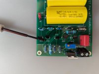
There was another suggestion in the thread that having some additional filtering of the voltage at the top of the output buffer might help also... see pic -- could try adding a bypass capacitor between that trace or directly at the drain of Q105 and ground... not sure what value would be appropriate though. I have a variety of values on hand... @ra7 any thoughts?
Attachments
I'm not convinced that what I've suggested there will solve anything, just brainstorming. A little more engineering is needed to gain a better understanding of the problem.
None of us know anything until we try!
ElArte - you are correct that there is a problem with the TOPPING dacs - I did use the CINEMAG transformers (1:1) on the "bass" channels to stop noise and because I needed the extra gain of the balanced output. Now I am using the FE2022 (how time flies) on the "bass" channel - instead of the transformer. I use the single ended out for the tweeter and the balanced for the bass. Both transformer or FE2022 stopped the noise problem. I have the FE2022 at one-half suggested gain. I have more gain than I know what to do with for the tweeters hence the single ended connection - plus I do think it sounds better.
On the original Big Buffer Board there was additional decoupling for the buffer but I never tried that one. It certainly was not extensive - just an additional capacitor.
I guess the question is which stage is causing the problem? I guess if there is interaction is there any other path than the power and ground? Does the circuit want a coupling cap between the two stages?
william2001, grounds are funny. I do not think you should sell your idea short.
I do not think I have ever heard of using two regulators in a two stage circuit ever making it worse.

Thanks Metaphile! This is great stuff. Good to get confirmation of the operation.
Yeah, this is interesting. I am clearly not seeing this performance without the buffer FETs removed. I recall Elarte was also getting higher distortion like me with the buffer bypassed but buffer FETs in place. Maybe he can confirm that.Yeah, if you look at my initial tests there's only a tiny difference in measured distortion with the buffer jumpered out versus with the buffer JFETS removed altogether, seems to me like evidence that clipping the leads or removing the buffer JFETs might not be necessary!
Something like 100 uF could be a start. But it should be coupled with some resistance to drain, say 100 ohms? That’s my next’s step for figuring out a solution.The ground plane on this board is huge, covers the whole bottom half, so I expect it's very low-impedance and I doubt running a home run wire back to the PSU ground input pin would make a substantial difference. It's an interesting idea though and I can maybe try it within the next week or so.
There was another suggestion in the thread that having some additional filtering of the voltage at the top of the output buffer might help also... see pic -- could try adding a bypass capacitor between that trace or directly at the drain of Q105 and ground... not sure what value would be appropriate though. I have a variety of values on hand... @ra7 any thoughts?
Something like 100 uF could be a start. But it should be coupled with some resistance to drain, say 100 ohms? That’s my next’s step for figuring out a solution.
I have a second board that still has the buffer FETs populated, I can try that on that one when I get a chance.
recall Elarte was also getting higher distortion like me with the buffer bypassed but buffer FETs in place. Maybe he can confirm that.
When I last tested, jumpering the buffer off circuit reduced distortion by a bit, but not much (TM).
If we are going to compare results it would be good to agree on an input level…because this preamp has quite a bit of gain and results will highly depend on input level.
I suggest 0.5V of input level as a reference point.
I am finishing up the headphones amp rebuild.
The new set-up has the R25 as the power source, which laughs at this load while standing upside down on one finger.
I configured it for 59V regulated because tombo56 said 60V is the limit and I don’t like to run anything at the limit.
I set 32.5V Vds on the preamp board.
I verified preamp board and headphones buffer board both a very steady 59.04V of voltage.
I am biasing the headphones buffer board at 80-85 mA this time around. It’s taking a bit of time because that board has 1R source resistors only.
For now, the jumper is set to include the output buffer.
I will measure again with the jumper set to exclude the output buffer.
Not cutting legs until we have more clarity on what’s going on.
Oh, I will measure this one out of the headphones buffer with a 50R load.
I want these results to be relevant to the use case.
I am anxious to see what I get with higher supply voltage, less noisy supply voltage, a single supply board which reduces a great deal of opportunity for minor current loops (as far as I understand it), higher Vds, higher bias of the headphones buffer.
Fingers crossed.
Next week, when the new donuts get in, I’ll resume work on the pure preamp build.
Initial results:

This is for my most difficult headphones at 100 db SPL...pretty loud, I very rarely listen at that level:
Vin 0= .34V
Vpp out = 7.35V
THD+N = 0.31%
THD = 0.24%
H2 = 0.24%
H3 = 0.01%

This is for my most difficult headphones at 105 db SPL..1 hour of this will damage my hearing:
Vin = 0.6V
Vpp out = 12.92V
THD+N = 0.54%
THD = 0.44%
H2 = 0.43%
H3 = 0.06%
So, basically, everything halved across the board.
What did it?
The new power supply?
The fact there is a single power supply eliminating potential current loops?
The fact the supply voltage is higher?
The fact that Vds is higher?
We won't know. Sorry.
More tests coming, but I need to take care of my Valentine now.
This is for my most difficult headphones at 100 db SPL...pretty loud, I very rarely listen at that level:
Vin 0= .34V
Vpp out = 7.35V
THD+N = 0.31%
THD = 0.24%
H2 = 0.24%
H3 = 0.01%
This is for my most difficult headphones at 105 db SPL..1 hour of this will damage my hearing:
Vin = 0.6V
Vpp out = 12.92V
THD+N = 0.54%
THD = 0.44%
H2 = 0.43%
H3 = 0.06%
So, basically, everything halved across the board.
What did it?
The new power supply?
The fact there is a single power supply eliminating potential current loops?
The fact the supply voltage is higher?
The fact that Vds is higher?
We won't know. Sorry.
More tests coming, but I need to take care of my Valentine now.
Last edited:
The THD seems to follow output swing. Am I seeing that right?
What would I guess about the sound from that description and measurements? I’d guess it sounds pretty sweet
What would I guess about the sound from that description and measurements? I’d guess it sounds pretty sweet
Last edited:
It seems like that. As previously, you can observe a few things:
1) Distortion level is flat across the frequency range.
2) Noise floor appears at the limit of what my instrument can measure. It may well be lower in fact.
3) It’s not clipping, even though the level of distortion is high-ish.
4) It’s pure H2.
That build is completely overhauled. Only the preamp board and the wires are identical to the previous version.
In retrospect, it reminds me of Papa’s harmonic generator:
https://positive-feedback.com/audio-discourse/the-pass-h2-harmonic-generator/
Read that, Rahul, there may be some clue in it.
I was really tired, so I didn’t listen for more than 30 minutes before doing a quick measurement.
It was Malia on Convergence.
It sounded very sweet!
OK, more tests...
The new headphones amp build:

The DC wiring will be better before I close the lid, bit I don't think it matters much, really.
Notice the electron tank on the R25 supply. That thing is nearly half the size of the transformer, which is the new transformer with 2 X 24V in series and static shield (purple wire).
As a first test and verify the validity on last night's initial tests:
Vin: 0.5V
Vout: 3.79 Vrms, 10.78 Vpp
THD+N: 0.47%
THD: 0.38%
H2: 0.37%
H3: 0.04%
Hard clip at 1.3 V of input.
Vds was at about 32.5V for yesterday's and this test.
Now, I jumpered off the output buffer.
Keeping Vds at yesterday's 32.5V.

Vin: 0.5V
Vout: 3.38Vrms, 9.6Vpp
THD+N: 0.23%
THD: 0.18%
H2: 0.18
H3: 0.03%
Hard clip at 1.5 V of input.
1 kHz spectrum:

100 Hz spectrum:

10 kHz spectrum:

So, obviously, bypassing the buffer seems to halve the THD in that build, which has 59V of R25-regulated supply.
Then, I decided to play with Vds...
At Vds = 35V

Vin: 0.5V
Vout: 3.37Vrms, 9.58Vpp
THD+N: 0.17%
THD: 0.13%
H2: 0.12%
H3: 0.03%
So, increasing Vds reduces THD further.
However, the THD is no longer ruler-flat across the FR.
At Vds = 33V

Vin: 0.5V
Vout: 3.36Vrms, 9.56Vpp
THD+N: 0.22%
THD: 0.17%
H2: 0.16%
H3: 0.03%
The THD is back to being ruler-flat across the FR.
1 kHz spectrum:

100 Hz spectrum:

10 kHz spectrum:

So, H2 at about -55 dB.
If I could supply 66V, this would probably be the sweet spot for this build, but I cannot.
I also tried 31V for Vds and 29.5V for Vds...THD increases as you decrease Vds. At my 59V of supply, Vds should be 29.5V to have symmetrical clipping.
For this build, it's all a matter of how much H2 I desire, Vds could be anything between 29.5 and 33V. The fact THD is not ruler flat at 35V tells me it's not quite right for this build.
I'll have to listen more and compare to see if I can actually tell the difference between 29.5V Vds and 33V Vds.
The new headphones amp build:
The DC wiring will be better before I close the lid, bit I don't think it matters much, really.
Notice the electron tank on the R25 supply. That thing is nearly half the size of the transformer, which is the new transformer with 2 X 24V in series and static shield (purple wire).
As a first test and verify the validity on last night's initial tests:
Vin: 0.5V
Vout: 3.79 Vrms, 10.78 Vpp
THD+N: 0.47%
THD: 0.38%
H2: 0.37%
H3: 0.04%
Hard clip at 1.3 V of input.
Vds was at about 32.5V for yesterday's and this test.
Now, I jumpered off the output buffer.
Keeping Vds at yesterday's 32.5V.
Vin: 0.5V
Vout: 3.38Vrms, 9.6Vpp
THD+N: 0.23%
THD: 0.18%
H2: 0.18
H3: 0.03%
Hard clip at 1.5 V of input.
1 kHz spectrum:
100 Hz spectrum:
10 kHz spectrum:
So, obviously, bypassing the buffer seems to halve the THD in that build, which has 59V of R25-regulated supply.
Then, I decided to play with Vds...
At Vds = 35V
Vin: 0.5V
Vout: 3.37Vrms, 9.58Vpp
THD+N: 0.17%
THD: 0.13%
H2: 0.12%
H3: 0.03%
So, increasing Vds reduces THD further.
However, the THD is no longer ruler-flat across the FR.
At Vds = 33V
Vin: 0.5V
Vout: 3.36Vrms, 9.56Vpp
THD+N: 0.22%
THD: 0.17%
H2: 0.16%
H3: 0.03%
The THD is back to being ruler-flat across the FR.
1 kHz spectrum:
100 Hz spectrum:
10 kHz spectrum:
So, H2 at about -55 dB.
If I could supply 66V, this would probably be the sweet spot for this build, but I cannot.
I also tried 31V for Vds and 29.5V for Vds...THD increases as you decrease Vds. At my 59V of supply, Vds should be 29.5V to have symmetrical clipping.
For this build, it's all a matter of how much H2 I desire, Vds could be anything between 29.5 and 33V. The fact THD is not ruler flat at 35V tells me it's not quite right for this build.
I'll have to listen more and compare to see if I can actually tell the difference between 29.5V Vds and 33V Vds.
Cool, thanks for that. The ones without buffer look pretty good. I can see why you aren’t in a rush to change anything 
I can see why you aren’t in a rush to change anything
The only irony is that I am doing back and forth tests between with and without buffer and I think I prefer it when the buffer is in!
The sound seems fuller, probably all that H2.
Could we run a wire between both FETs pin 1? Seems like the simplest way to do this. Would this cause I problem I do not know about?
I presume you mean the two rightmost pins? Those are the drains, one connected to power, other to ground. Don’t want to short that. Just leave as is for now. Both Metaphile and Elarte’s measurements are very good. In the meantime, I’ll work on figuring out a solution.
Alright, some interesting new measurements.
Since I have two boards, one with Q105 and Q106 installed and one with them removed, I switched to the one that still had the buffer installed (at first).
Conclusions:
Measuring setup:
Also, the biggest impact on the distortion numbers came from increasing the Vd - a bigger impact at these higher swings than merely jumpering out or even removing the buffer JFETs.
Hope that's all interesting. For my part, I intend to remove the buffer JFETs from both of the board when I install these into my TDV amp and set the Vd to 40V. I'm quite pleased that I can get 0.52% distortion from the preamp stage of the amp at nearly 20W into 8 ohms, which would exceed the capability of the TDV amp anyway.
Since I have two boards, one with Q105 and Q106 installed and one with them removed, I switched to the one that still had the buffer installed (at first).
Conclusions:
- At the same Vd operating point, jumpering out the buffer versus removing it makes little-to-no measurable difference.
- The buffer seems to add about .1% distortion at the 9Vrms output level.
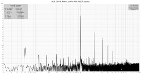
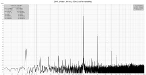
- Adding a 100uF bypass capacitor to the V+ rail at the drain of Q105 makes no measurable difference.
- The biggest reduction in distortion resulted from raising the Vd operating point, I tested up to 40Vd. Removing the buffer JFETs allowed me, with the same power supply, to get higher maximum output voltage from the preamp at operating point Vd's above 30V and 35V.
- Recommendation: remove the output buffer JFETs from the board unless you need to drive a challenging load, and increase your Vd operating point to 40V to get lower distortion from this preamp. Operating point versus maximum output voltage can be a compromise, depending on your input voltage. Mine is 60.4V.
Measuring setup:
- Now using the 10:1 step down with 1M / 100k divider on the output into the Focusrite
- Measuring at 9Vrms per @ra7 's suggestion
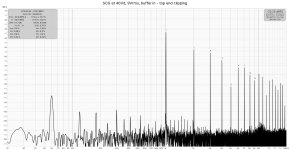
- With the buffer JFETs installed, and setting the Vd to 40V, I couldn't get 9Vrms without the top end of the waveform flattening (first attachment, 13.7% THD at 9Vrms.) I had to lower the Vd to 30V for the next set of measurements to get a 9Vrms output without clipping the positive cycle of the waveform.
- I tried adding a bypass capacitor - 100uF with a 100ohm resistor - between ground and the drain of Q105 (the JFET at the top of the buffer circuit). This made no difference at all the the THD, which was 1.11% at 9Vrms with the buffer enabled.
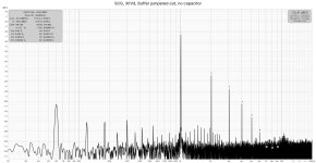
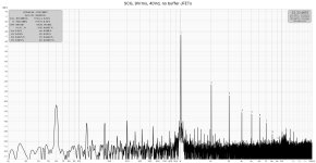
- I then disabled the buffer - THD at 9Vrms dropped to 0.99%.
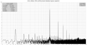
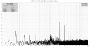
- Then I raised the Vd from 30V to 35V - this reduced the THD at 9Vrms to 0.60%. I tried both with and without the bypass capacitor to the drain of Q105. This made no difference in distortion.
- Re-enabling the buffer via the jumper, with the Vd still at 35V - the distortion again increased to 0.69%.
- Starting at 35Vd to compare to the measurement above (ignore the "3Vd" on the screenshot, that's a typo), I got identical performance - 0.59% THD.
- Now, with the buffer JFETs removed, I was able to increase the Vd to 40V without clipping the top half of the waveform. Distortion dropped to 0.34%.
- Later, I found that at the 40Vd operating point, I was able to reach 12.6Vrms (or 36Vpp) at only 0.52% THD.
Also, the biggest impact on the distortion numbers came from increasing the Vd - a bigger impact at these higher swings than merely jumpering out or even removing the buffer JFETs.
Hope that's all interesting. For my part, I intend to remove the buffer JFETs from both of the board when I install these into my TDV amp and set the Vd to 40V. I'm quite pleased that I can get 0.52% distortion from the preamp stage of the amp at nearly 20W into 8 ohms, which would exceed the capability of the TDV amp anyway.
Attachments
-
 21-SCG-divider-9vrms-bypass-1-11thd.jpg313.3 KB · Views: 23
 -
 22-SCG-divider-9vrms-bypass-0-98d.jpg312.5 KB · Views: 25
 -
 23-SCG-divider-9vrms-bypass-061thd.jpg312.4 KB · Views: 27
 -
 24-SCG-divider-9vrms-buffer-069thd.jpg309.8 KB · Views: 20
 -
 26-SCG-divider-9vrms-nobuffer-033thd.jpg311.6 KB · Views: 29
 -
 25-SCG-divider-9vrms-nobuffer-060thd.jpg312 KB · Views: 20
 -
 20-SCG-divider-9vrms-13-7thd.jpg322.5 KB · Views: 22
- Home
- Amplifiers
- Pass Labs
- Schade Common Gate (SCG) Preamp