I bought a SOLDA-PULT years ago - maybe it works on large "holes" - but the holes for the FETs - especially with 2 mm PCBs - I doubt it will work very well. One would need a stronger vacuum and one that would last long enough to do the job.
This might be as cheap as it gets for something that will likely work:
https://www.amazon.com/Hakko-FR-301...fix=desoldering+station,industrial,113&sr=1-6
That is one hell of an address.
https://www.amazon.com/Hakko-FR-301...fix=desoldering+station,industrial,113&sr=1-6
That is one hell of an address.
Another thought - it would probably be easiest of all to just cut the power trace on the PCB which would be easy to enough to jumper in the future if needed.
I am at work so I do not have one in front of me but I cannot imagine this being tricky.
I am at work so I do not have one in front of me but I cannot imagine this being tricky.
This might be as cheap as it gets for something that will likely work:
https://www.amazon.com/Hakko-FR-301...fix=desoldering+station,industrial,113&sr=1-6
That is one hell of an address.
After struggling with the cheaper alternatives and damaging too many old boards and traces, I purchased one of those.
I have absolutely no regrets. Can recommend buying a second larger 1.2mm tip for desoldering large pinned things like heatsinks and potentiometers. Also, you really gotta keep up with the maintenance. My only complaint with it, life changing though it is, is that it doesn't automatically power off and the indicator light is on the handle. So I have, recently, accidentally left it on at the maximum temp setting for weeks at a time. Which oxidized a brand new tip almost beyond recovery.

On the small board it looks like cutting the trace on the side near R105 - cut between the R105 and Q105 would stop the B+ along with removing R107 which would be simple in comparison to removing the FETs which might be useful in the future.
Unless there is something I do not know which is always entirely possible - I see no need to worry about cutting the ground.
I am not using the output capacitor on the board - going from the "square" hole of the jumper out to the input cap for the amplifier.
To retain the cap run a jumper from the right hole of the vacated R107 to the middle of the jumper. I will take my output from this point to the cap at the amplifier.
Good to hear metaphile has found this device to work. One can never have enough tools for this audio mania we have.
I found it easiest to snip the drain pins of the jfets and leave them in place otherwise. Can be reverted with a small jumper later if needed. It takes less than a minute.
Apologies to you all (@ElArte @metaphile @rickmcinnis and others) who built the boards. I took a long time to finalize the design and it is frustrating to have to change built boards. I am frustrated with myself because I put in a lot of time into the final design only to miss this aspect. Thankfully, the preamp functions fine without changing anything and it sounds good. And that is part of the reason why it went undetected.
The Soldapult tool did it for me and I am no longer afraid of desoldering. The Hakko looks like the ultimate solution !
As one learns from EQing speakers - there are always many ways to skin the cat.
I worry about "jumpering" the FETs - to each his own.
No need for any apologies, Rahul. Your work is appreciated. I have no complaints at all. This whole thing has been a great and worthwhile adventure.
If you could get the Solda-pult to work with TO92 holes I am only in more awe of your abilities!
I worry about "jumpering" the FETs - to each his own.
No need for any apologies, Rahul. Your work is appreciated. I have no complaints at all. This whole thing has been a great and worthwhile adventure.
If you could get the Solda-pult to work with TO92 holes I am only in more awe of your abilities!
i think I have come around to Rahul's method of clipping the leads. Won't be that hard to re-attach.
I keep thinking about william2001's: "Like maybe try lifting pin 1 of Q106 from the ground plane, and run a wire from that guy straight to the PS_IN_GND. Preferably in close relation to the feed line (Q105 pin 1 trace) to minimize the loop area. Just an idea... (and I'm running out of those). Will be interesting to see what solves this issue".
I think of tombo's regulator where he made mention that he deliberately did not allow the ground plane to cover the entire board. Which is what william2001 is talking about. For lack of the proper word and my lack of knowledge - grounds need to be "zoned".
I have to say (again) I do have admiration for tombo's R25. I think he knows a great deal about pcb layout.
Just a rumination after a few cocktails ...
First off, please don't apologize. We all appreciate the work and the time you put into this project, and we're all here to have fun and experiment, after all.
I set up the preamp and took some distortion measurements tonight; you may find my findings interesting.
First of all, baseline setup:
- I am using @ra7 's regulated power supply board with a Hammond 166G50 power transformer. That's a 50VAC single CT secondary @ 500mA. My Zener string is made up of 3x 20V Zeners and 1x 6.2V Zener and I get 60.4VDC into the SCG preamp. I tried raising the supply voltage by swapping the 6.2V Zener for a 15V Zener; this gave 69.4V but there was a significant amount noise on the output of the preamp (~30mV if I recall correctly), so I reverted back to the 20-20-20-6.2V zener string. Noise went away. Probably need more headroom from a beefier transformer to get a less noisy result around 70V+; opinions welcome.
- Per @ra7 's suggestion I set the operating point at 35VDC. I noticed it comes up slowly as the preamp warms up so I gave it some time to settle in.
- I'm using an Akitika 1Khz oscillator to generate the test sine wave.
- I'm using a Focusrite Scarlet 2i2 and REW to measure distortion.
- Measuring across a 10K resistor at the output of the preamp. Scope to measure signal amplitude, Focusrite to measure distortion.
Buffer in place, baseline measurements:
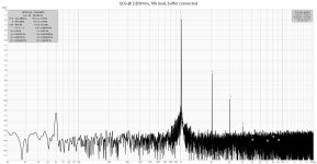
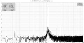
- First measurement was 2.83Vrms with the buffer in place and the jumper set to enable the buffer. 0.19% THD, predominantly second harmonic.
- Second measurement I set out to find the max output before clipping. At 8.92Vrms, 0.65% THD, still predominantly second harmonic. (From here, increasing the input signal even a tiny bit immediately shot the distortion way up to around 5%.)
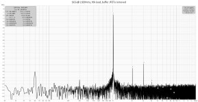
- Third measurement I moved the jumper to the buffer bypass position and took another measurement at 2.83Vrms. Now THD has dropped by over 10x, 0.015%, slightly greater 3rd harmonic.
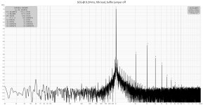
- Fourth measurement I set out again to find the max output before clipping. Now, at 9.2Vrms, I reached 0.15% THD - less distortion than I measured at only 2.83Vrms with the buffer enabled! Still predominantly 3rd harmonic now with some higher harmonics present. (Once again, I couldn't increase the input signal by even a tiny bit before the distortion shot up from here).
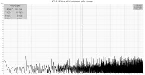
- Fifth measurement was again 2.83Vrms and now, slightly better performance with no buffer at all: 0.013% THD, predominantly 3rd harmonic.
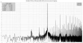
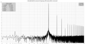
- Sixth measurement, looking for max output before clipping with no buffer JFETS, I was able to get 9.77Vrms before crossing the 1% THD line. Lots of higher harmonics, we are beginning to clip here. Not a very meaningful difference from what I found with the buffer bypassed, maybe a few tenths of a volt extra output.
That said, I'm very curious why I'm not getting nearly as much usable voltage swing (taking the 1% clipping figure, I'm getting 27.6Vpp) as @ra7 -- any ideas? Input voltage of 60.4V too low for those big numbers, I presume? 35VDC operating point needs some tweaking?
While I'm here - should I consider running these dual mono with two power supply boards and two transformers? Seems mega-overkill for a preamp that only draws 15-20mA but I'm curious.
Attachments
-
 01-SCG-10k-2-38vrms-019THD.jpg315.8 KB · Views: 36
 -
 06-SCG-10k-976Vrms-1thd.jpg342.7 KB · Views: 31
 -
 05-SCG-10k-2-83vrms-0013thd.jpg314 KB · Views: 38
 -
 04-SCG-10k-9-20vrms-015thd.jpg315.8 KB · Views: 36
 -
 03-SCG-10k-2-83vrms-0015thd.jpg313.3 KB · Views: 37
 -
 02-SCG-10k-28-93vrms-065THD.jpg323.8 KB · Views: 34
Last edited:
Very interesting. Thanks for sharing! Can you keep the distortion measurement running and move Vd upwards towards 40V? What happens to THD and max swing?
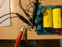
Oh wait, it might be the ADC is clipping. I use a 1:10 stepdown to measure above 10Vrms, coz my ADC clips above that. Even getting near 10Vrms it starts becoming gnarly. You can build an easy step down as follows: from output + connect a 1Meg resistor and a 100k resistor to ground. Other end of 1Meg connects to the ADC.
I then connect an RCA jack at the other end to feed the ADC and use clips to connect the input of this step down to the preamp output. So, in the image below, the white clip goes to preamp out, and black to preamp ground.
Also, the soundcard input should be 10k, so you can leave off the separate 10k resistor when measuring without the stepdown.
The max input on the Scarlet 2i2 is 22 dbu, which is 9.75 Vrms. So, it checks out  . The step down will do it.
. The step down will do it.I finished building a R25 tonight and ran some initial tests. Very nice.
Of course it’s quite overkill for my headphones amp build that draws less than 0.5A, but I won’t have to worry about stressing resistors while regulating 58-60V.
I also ordered more donuts for the preamp build.
I am still on the fence about desoldering the output buffer in either build.
Of course it’s quite overkill for my headphones amp build that draws less than 0.5A, but I won’t have to worry about stressing resistors while regulating 58-60V.
I also ordered more donuts for the preamp build.
I am still on the fence about desoldering the output buffer in either build.
Apologies to you all (@ElArte @metaphile @rickmcinnis and others) who built the boards. I took a long time to finalize the design and it is frustrating to have to change built boards. I am frustrated with myself because I put in a lot of time into the final design only to miss this aspect.
No need to be sorry.
It’s DIY, Rahul. I know what I am getting into every time I am an early builder.
And I still think it sounds good with all that H2. Hence my hesitation to make the change.
Buffer JFETs desoldered and removed from the board:
- Fifth measurement was again 2.83Vrms and now, slightly better performance with no buffer at all: 0.013% THD, predominantly 3rd harmonic.
- Sixth measurement, looking for max output before clipping with no buffer JFETS, I was able to get 9.77Vrms before crossing the 1% THD line. Lots of higher harmonics, we are beginning to clip here. Not a very meaningful difference from what I found with the buffer bypassed, maybe a few tenths of a volt extra output.
😭 My precious H2!
Hopefully it’s the ADC clipping it.
Hey @ra7 - you were right; I was clipping the Focusrite input. Good catch!
I think we're witnessing the limitations of the measuring equipment.
I made the change you suggested and adjusted the Vd from 35V->40V. I watched the distortion decrease in real time when I did this. I also was able to get a much higher output voltage before clipping (12.6Vrms) than before. I can see the top side of the waveform start to clip on the scope when I go higher than that. This is about 36Vpp, much closer to the expected 40Vpp.
Weirdly, though, the distortion measurements at 2.83Vrms increased and the distortion character changed. I can only assume this is the affect of the voltage divider or some other quirk of the measuring setup - because I noticed that increased number even before I adjusted the Vd to 40V (which decreased it from something like 0.15% to 0.11%).
Anyway it's late here on the East coast so I'm off to bed. I should have some more time this weekend to experiment.
Attachments

metaphile - since you are adept at measuring - would it be possible for you to try william2000's idea?
I have always used one supply/regulator per channel but I do not think that solves the problem. Maybe using two of the boards for each channel and going beyond william2000's suggestion would be the ultimate solution. The additional board connected to each buffer FETs pin one. It would be slightly awkward packaging but if you saw my system you would know it would fit right in!
If the circuit worked well in Rahul's sim it has to be basically right and it makes sense that it is a grounding problem.
I have always used one supply/regulator per channel but I do not think that solves the problem.
You said you are using Topping DACs or the like, right? These sources connect both channel signal ground together and to earth ground via a low impedance path (I do not know how). So, unless you use 1:1 input transformers, your preamp grounds won't be isolated. (You might want to forget I ever said this; as I have been trying to do for a few weeks now. Transformers have their own problems, no doubt.)
Maybe using two of the boards for each channel and going beyond william2000's suggestion would be the ultimate solution.
I am not sure I understand this, as signal ground and power do meet on the preamp board anyhow.
I think william2000's suggestion was more about avoiding a large ground plane on the preamp board. I think he was advocating for 2 planes connected by a > 0 impedance path.
I could be wrong, I am really stretching what I have learned about this.
I think we're witnessing the limitations of the measuring equipment.
I acknowledge my equipment's limitations - it cannot accurately measure THD below 0.01%.
In your previous report, you noted minimal difference between the output buffer being jumpered off versus completely removed. This seems to contradict Rahul's findings (where modulation occurred unless the JFET drains were disconnected). This discrepancy warrants further investigation.
I'm still hoping to avoid any desoldering... heh.
I hope to minimize it or if we do have to cut some way to maintain the buffer. On the one channel I have using the buffer it does seem have some beneficial affects.
Until I get the other channel finished it is hard to be sure. That will happen Saturday.
Still keep pondering william2001's (was one year shy in my previous post) idea as a minimum to be given a try.
El Arte - from memory the ground plane covers the entire board - I am speaking of the small one channel board. I guess you are using JUMBO and I have no idea on that one. BUT if that is the case that could well destroy my surmising!
- Home
- Amplifiers
- Pass Labs
- Schade Common Gate (SCG) Preamp