I think I solved the puzzle of why the distortion is higher compared to my old measurements. It is the output buffer. More coming tonight.

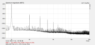
This thing was driving me absolutely nuts. Why did the measurements from ElArte and Metaphile show high levels of distortion? Why didn't the output make it to 40Vpp? My original measurements in post #1337 showed about five times lower distortion and uninhibited output swing. I measured up to 60Vpp swing back then.
It turns out there is some sort of modulation of the CCS or another node in the preamp stage from the output stage. This seems odd because it does not show up in an LTSpice model and because the output buffer devices have their drains pointed to the supply. FET drains are high impedance per my understanding, so I am still not sure exactly what is going on and how the input is being modulated by the output (oscillation? not enough decoupling?). Even after I disconnected the output bias resistors R107/108 there was still modulation. Really puzzling.
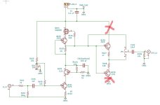
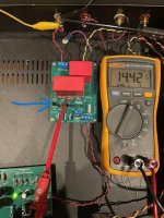
But the solution is simple: disconnect the output JFETs. You can simply disconnect the drain pins and that will be enough. Next, turn up the Vd to 35V (if your supply can go higher, then turn up Vd further, up to 45V). That's it. Looking at the board from the power supply input side (see pic below), the output JFETs are the two critters all the way to the left of the board. Q105 and Q106. The rightmost pins on each of them are the drain pins and should be disconnected.
Here's a pic and a measurement and also confirming via schematic the pins to be disconnected.
Frankly, I am embarrassed that this got through to the final design. I'll triple check the measurements next time before finalizing the design and I did that for the first two iterations. I was just enjoying the sound too much--likely because my output swing is not that high. But no, this is the performance that I promised.
@ElArte @metaphile, could I ask you to please check the measurements after this change? I'd very much appreciate it.
The preamp works fine without the buffer and, in fact, there is a provision on the PCB to use it without the buffer (the jumper). The measured response below is into a 10k load. It will drive the F4 absolutely perfectly, and other amps with not too low an input impedance will also be totally fine. My objective with the buffer was to drive high impedance headphones directly and also drive the lateral FET MOFO, which does need a bit more oomph and drive.
Some sort of decoupling of the drains from the gain stage CCS could work. I need to test it, but at least we have the original performance back. Phew!
It turns out there is some sort of modulation of the CCS or another node in the preamp stage from the output stage. This seems odd because it does not show up in an LTSpice model and because the output buffer devices have their drains pointed to the supply. FET drains are high impedance per my understanding, so I am still not sure exactly what is going on and how the input is being modulated by the output (oscillation? not enough decoupling?). Even after I disconnected the output bias resistors R107/108 there was still modulation. Really puzzling.
But the solution is simple: disconnect the output JFETs. You can simply disconnect the drain pins and that will be enough. Next, turn up the Vd to 35V (if your supply can go higher, then turn up Vd further, up to 45V). That's it. Looking at the board from the power supply input side (see pic below), the output JFETs are the two critters all the way to the left of the board. Q105 and Q106. The rightmost pins on each of them are the drain pins and should be disconnected.
Here's a pic and a measurement and also confirming via schematic the pins to be disconnected.
Frankly, I am embarrassed that this got through to the final design. I'll triple check the measurements next time before finalizing the design and I did that for the first two iterations. I was just enjoying the sound too much--likely because my output swing is not that high. But no, this is the performance that I promised.
@ElArte @metaphile, could I ask you to please check the measurements after this change? I'd very much appreciate it.
The preamp works fine without the buffer and, in fact, there is a provision on the PCB to use it without the buffer (the jumper). The measured response below is into a 10k load. It will drive the F4 absolutely perfectly, and other amps with not too low an input impedance will also be totally fine. My objective with the buffer was to drive high impedance headphones directly and also drive the lateral FET MOFO, which does need a bit more oomph and drive.
Some sort of decoupling of the drains from the gain stage CCS could work. I need to test it, but at least we have the original performance back. Phew!
Attachments
Last edited:
The only other thing I'd recommend is upping the power supply voltage to 70-75V. You can get there by using this Antek power toroid with twin 32V secondary windings and connecting the secondary windings in series to get a single 64V secondary. I bought two.
https://www.antekinc.com/an-0232-25va-32v-transformer/
With this donut and a fourth 18-20V zener on the PS board, I am getting 70-75V. Then you can turn up the Vd to 40V.

https://www.antekinc.com/an-0232-25va-32v-transformer/
With this donut and a fourth 18-20V zener on the PS board, I am getting 70-75V. Then you can turn up the Vd to 40V.
Last edited:
Cutting those legs would be a no return thing. (I didn't note the matched values of the JFETs.) Cutting the trace even more so. I don't think I'll do that in the headphones amp version.
Since the jumper allows taking out the output buffer, isn't that a better way to go?
I may try that in the preamp build.
As for boosting the to 64V of AC input to the supply boards, it would require an adjusted snubber, filter caps with more margin, and zener string changes...pretty much new boards at that point...I don't think I can do this right now. Maybe at the end of the year.
I will have close to 60V out of the supply boards, and I have resigned myself to that.
Even with the higher distortion, I love what I have.
I'd be happy to try this experiment (I may even have some time tomorrow - or if not, this weekend) and even take some distortion measurements before and after.
I will mention though that I didn't post any distortion of the SCG earlier - just shared that I was only seeing far less maximum voltage swing than expected.
But I have a question for you, Rahul, since you also designed the TDV, which is the intended application for my SCG preamp boards. Do you think the input impedance of the TDV (I'm using a 10k resistor to ground at the input without any apparent bias instability, though I know some had to use a lower value to get stable bias) is high enough that the buffer is not required? I also have the same question as ElArte, should I just jumper out the buffer stage rather than disconnecting the JFET drain pins or otherwise?
This data point might not be particularly relevant, since it is a cumulative distortion measurement, but FWIW I measured 0.16% THD with the SCG driving a TDV follower output stage at 1W (2.83Vrms). The other channel, different SIT, 0.25%. Prior to adding in the SCG I did a test measurement with the SIT in a common source configuration also at 1W/2.83Vrms and measured only 0.02%. So indeed it seems the distortion contribution of the SCG is higher than expected with the buffer connected?
I think I answered both of my own questions...
If your measured results were into a 10k load then the input impedance of my TDV should show similar performance given that the 10k resistor at the input pretty much sets the input impedance.
And I'm guessing the reason the pins must be disconnected rather than simply using the jumper is that they're driven by the input signal regardless and so the same modulation may occur regardless of the jumper position?
I'll try this experiment and report back. I have a desoldering gun so my job is easy. I'll remove the output buffer FETs and change the jumper position.
Right now I'm playing with a ~60V supply but the transformer I ordered should be able to give me a bit closer to 70V, will try that too once I have received it.
All that said, I'm in no need of massive amounts of swing since the TDV at the voltage and bias points I'm considering can only produce about 10W so I'm more interested in the effect on the distortion than achieving massive voltage swing (at least until I have an F4 on hand to drive).
With this modulation even with the output bias resistors removed... does this also happen if Q106 is removed?
And you could be right about needing some decoupling. Perhaps some C at the R105 / RV1 string, or even an RC. Particularly with the PS regulator living some distance away from the load as I look at these builds..
Yeah, that might do it. Needs to be tested. I was trying to keep the buffer output impedance low and so didn’t add any resistance to the drain. But maybe a little bit of resistance on the three branches and some capacitance will cure it. I did try adding capacitance to the voltage divider on the input but that didn’t help.
Even with the jumper connected to the gain stage output, there is modulation. In your applications, cutting off the drains of the buffer should have no impact. You are using the headphone buffer to drive headphones and the preamp will drive other amps just fine.Cutting those legs would be a no return thing. (I didn't note the matched values of the JFETs.) Cutting the trace even more so. I don't think I'll do that in the headphones amp version.
Since the jumper allows taking out the output buffer, isn't that a better way to go?
If you used the BOM, it has 100V caps, so simply swapping out the trafo works. If you are up to 60V, you should be good already. No need to change. Just up the Vd to 35-40V.I may try that in the preamp build.
As for boosting the to 64V of AC input to the supply boards, it would require an adjusted snubber, filter caps with more margin, and zener string changes...pretty much new boards at that point...I don't think I can do this right now. Maybe at the end of the year.
Yeah, the distortion is innocuous because it is second order. Fooled me too.I will have close to 60V out of the supply boards, and I have resigned myself to that.
Even with the higher distortion, I love what I have.
You got it!I think I answered both of my own questions...
Yes, it will drive the TDV just fine.If your measured results were into a 10k load then the input impedance of my TDV should show similar performance given that the 10k resistor at the input pretty much sets the input impedance.
60V supply works fine with 35-40V Vd.Right now I'm playing with a ~60V supply but the transformer I ordered should be able to give me a bit closer to 70V, will try that too once I have received it.
Makes sense. But I bet removing the output JFETS will make a difference. Curious to hear before and after sound impressions too.All that said, I'm in no need of massive amounts of swing since the TDV at the voltage and bias points I'm considering can only produce about 10W so I'm more interested in the effect on the distortion than achieving massive voltage swing (at least until I have an F4 on hand to drive).
I have one channel with the new setup using the buffer - 35 volts - and it sounds a little more lively - but that could well be from the selection process for the other FETs and your PCB layout.
I have had the thought that - the left side sure sounds good even though it is the old style - so I am not the least surprised at this. Simple is damned hard to beat. But I am intrigued with the thought of the possibility of an even more effortless sound with the buffer.
Does the buffer need its own current source? I ordered lots of boards and could easily make a two board setup - one for the main circuit and one for the buffer each having a current source of their own. Any chance that would do any good?
In the interim - it would seem important to keep the buffer FETs from consuming power so simply using the non-buffer output would not be sufficient?
The path to audio nirvana is a rocky one ...
The buffer is a classic push-pull output stage. See the last stage in Wayne’s P3 or the F4, for example. So, it doesn’t need a CCS. It provides a low-impedance drive and more current for hungry output devices, such as lateral FETs. But for driving an F4, which already has an input buffer, it is not needed. And first, it needs to start behaving more politely towards the input stage.
Makes sense. But I bet removing the output JFETS will make a difference. Curious to hear before and after sound impressions too.
I have no listening impressions to share yet because I haven't hooked the setup to speakers just dummy loads and measuring instruments. 🤓
But I will let you know if I hear any noticeable difference on my cheap bench-top speakers when I make the change.
Hmm, possibly some circulating currents causing some contamination in the ground plane? In some cases isolating different sections of the ground plane might be necessary to prevent cross-contamination. Like maybe try lifting pin 1 of Q106 from the ground plane, and run a wire from that guy straight to the PS_IN_GND. Preferably in close relation to the feed line (Q105 pin 1 trace) to minimize the loop area. Just an idea... (and I'm running out of those). Will be interesting to see what solves this issue.
I have no listening impressions to share yet because I haven't hooked the setup to speakers just dummy loads and measuring instruments. 🤓
But I will let you know if I hear any noticeable difference on my cheap bench-top speakers when I make the change.
This situation seems very fluid.
Let me know what you find out before I make any irreversible changes.
This tool makes desoldering a breeze:
https://a.co/d/166wgQY
Recommended by Papa himself when I made a gaffe with the Sony VFETs. It is ridiculous how good it is. A little bit of fresh solder to get the joint flowing really helps, and then that tool sucks it all in.
https://a.co/d/166wgQY
Recommended by Papa himself when I made a gaffe with the Sony VFETs. It is ridiculous how good it is. A little bit of fresh solder to get the joint flowing really helps, and then that tool sucks it all in.
I am running mine straight into the THF51 TDV style so I have no idea how this compares to an F4.
I was thinking of the CS as nothing more than an isolation device more than something the buffer needed to perform at its best.
Maybe a separate power supply instead of the CS? That would be pretty easy to do.
I was thinking of the CS as nothing more than an isolation device more than something the buffer needed to perform at its best.
Maybe a separate power supply instead of the CS? That would be pretty easy to do.
This tool makes desoldering a breeze:
https://a.co/d/166wgQY
Recommended by Papa himself when I made a gaffe with the Sony VFETs. It is ridiculous how good it is. A little bit of fresh solder to get the joint flowing really helps, and then that tool sucks it all in.
Will order.
I endeavor to get good flow through while soldering, which is great, but the time comes to desolder, it’s a nightmare.
I have ruined many boards trying various ways.
- Home
- Amplifiers
- Pass Labs
- Schade Common Gate (SCG) Preamp