Have you made even a first attempt to determine that the J113 FET's have a suitable noise performance?
Have you made even a first attempt to determine that the J113 FET's have a suitable noise performance?
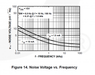
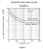
It's right there in the datasheet. The noise performance is broadly comparable using an audio op amp for the same purpose. A little better at high frequency, the same or perhaps a little worse at low frequencies. I've shown a bipolar op amp by way of example, a FET input type like the OPA134 is a little worse again.
Attachments
Last edited:
It's right there in the datasheet. The noise performance is broadly comparable using an audio op amp for the same purpose. A little better at high frequency, the same or perhaps a little worse at low frequencies. I've shown a bipolar op amp by way of example, a FET input type like the OPA134 is a little worse again.
I meant actually measure a few typical samples. They are not speced for audio and other Fairchild switches need to be screened for audio frequency noise i.e. the spec is typical not guaranteed. For some parts the opposite is true the data sheet looks bad but the yield to low noise is excellent, BF862 for instance.
Last edited:
Hi Scott,
That the J113 is marketed as a switch was a area of concern. We'll just have to see how it plays out, while hoping that the datasheet is a reasonable approximation of actual performance.
I certainly will be able to confirm the noise floor once I have the first prototype running. This should be in a week or so.
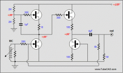
This would interest you.
http://www.tubecad.com/2004/AikidoAmp12.gif
Aikido Tube Amplifiers
It has good PSRR without using a CCS.
Instead it feeds the PS noise to both top & bottom FET of the follower for self cancellation.
Very clever.
Patrick
http://www.tubecad.com/2004/AikidoAmp12.gif
Aikido Tube Amplifiers
It has good PSRR without using a CCS.
Instead it feeds the PS noise to both top & bottom FET of the follower for self cancellation.
Very clever.
Patrick
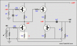
Ok, real quick: a sketch-up of the circuit in the previous post.
note the original circuit is missing the source resistor on the input jfet, I, uh, took the liberty of fixing that. 🙂
(You can also deconstruct the circuit back to the CrystalFET by removing the two CSS stages. You can see the distortion is very similar. Basically what you get for your pains is about 12 dB of PSRR and the ability to run at much lower supply voltages.)
Attachments

Last edited:
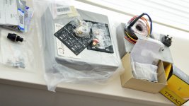
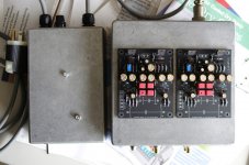
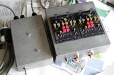
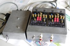
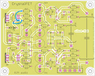
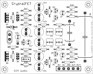
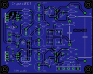
Prepared the CrystalFET chassis and power supply.
I hate this part of the process - drilling holes - but at least it's over with. The power supply is up and running, I just have to finish the boards and do the internal hookup.
I hate this part of the process - drilling holes - but at least it's over with. The power supply is up and running, I just have to finish the boards and do the internal hookup.
Attachments
> I like the look of the other variant even more.
You will change the sonic signature using a high NFB as that one.
Might as well use an opamp then.
Patrick
You will change the sonic signature using a high NFB as that one.
Might as well use an opamp then.
Patrick
It's only about 12 dB of global feedback. But on a wider front I absolutely agree with you: some circuit topologies are best kept for what they are, optimized with only a light hand. Throw in the kitchen sink to "improve performance" and the results rarely satisfy.
It's only about 12 dB of global feedback. But on a wider front I absolutely agree with you: some circuit topologies are best kept for what they are, optimized with only a light hand. Throw in the kitchen sink to "improve performance" and the results rarely satisfy.
Richard your tenacity is impressive, I haven't been to Kyoto in years I miss the local kaiseki the best in Japan IMHO.
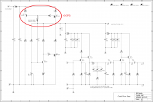
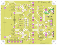
Oops!
I made an error when transferring the LTspice circuit to Eagle.
Boards need a re-spin. The fix is easy enough, but doing another run will take some time.
Existing boards can be fixed with a trace cut and a couple of flying leads.
I made an error when transferring the LTspice circuit to Eagle.
Boards need a re-spin. The fix is easy enough, but doing another run will take some time.
Existing boards can be fixed with a trace cut and a couple of flying leads.
Attachments

Last edited:
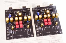
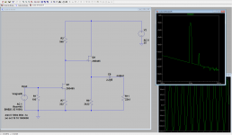
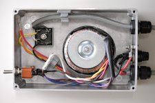
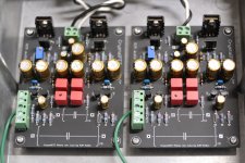
And here it is powered up, DC bias operational state but no signal wiring.
Mosfet regulator section works as expected. R20 full CCW V+ is about 15-20 V, adjusts to 35 V after a few turns CW. Output voltage falls about 1~1.5 V after being powered up for a few minutes. Current source output 30 mA, about 20% less than simulation, probably because the transistors used are different types.
I found the jfets bias a little hotter current than calculated, pulling the drain voltages to between 7~8 V when 9~10 V was calculated. I'm not sure why, but it's pretty close and can be easily redressed by decreasing R2 and R8 a little.
Attachments
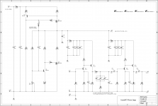
This is rev. 1.2a, with the corrected schematic.
Q5 is rotated 180 degrees, and R15 and R16 have had their parts values exchanged. There are no other changes.
Q5 is rotated 180 degrees, and R15 and R16 have had their parts values exchanged. There are no other changes.
Attachments
- Status
- Not open for further replies.
- Home
- Source & Line
- Analogue Source
- RJM Audio Crystal P jfet phono preamplifier | development thread