Another question. The J111, J112, J113 are invariably binned out of the same basic part, this is the way Fairchild does it as opposed to Toshiba, etc. with their color dot gradings. The J113 is speced at min Idss of 2mA. Your sim file shows Beta for J113 at 13m and 80m in my experience this is not possible with any process I have ever seen, not in 40yr. There is an error somewhere, some of these low Ron switches deviate a lot from square law behavior so possibly your two sample points are too close together and catch the wrong slope.
Attachments
Last edited:
I think I've found the root of the problem.
The jfets I used in my build were ones I measured and binned early on, before I added the bypass capacitor to the measurement circuit. There seems to have been some oscillation which threw off the DC voltage measurement by a small amount. Enough to get a wrong estimate for Idss and Vgs0 but unfortunately not wrong enough for me to pick up on it outright.
(later I changed the layout and the oscillation was obvious, at which point I clued in and added the capacitor... but I neglected to consider that the first layout, which seemed to give the right values, would also have been affected.)
I can't remeasure the ones in my boards, but I did remeasure some from the same batch,
original (typ): V1 0.921 V2 0.730, Vgs0 1.47 Idss 19.8
redo (typ): V1 0.998 V2 0.800, Vgs0 1.60 Idss 21.3
The pinch off voltages are a little higher. Assuming the ones I used were affected in the same way, it would explain why I only see 51-52 dB gain (and why Vds is lower than expected).
I backed out the probable values of the jfets I used from the gain and DC bias points to be Vgs0 1.64 V and Idss 12.5 mA, not 1.35 V and 23-27 mA as I originally thought.
The beta values for a few samples I checked seems to be in the range of 4-10m.
I agree that if the devices don't follow the expected square law I'm going to have to re-think this completely.
Attachments
Last edited:
additional:
If the most recent measurements are correct (which seems to be borne out by the actual measured gain and DC operating points of the circuit) then,
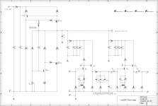
1) The moving magnet configuration will have to be modified to add partially bypassed source resistors which would allow the gain to be set around 35-40 dB. See attached schematic for how this could be done. While the changes can be made on the existing boards by flying leads and some creative 3D component placement, a re-spin will be needed to implement it properly.
2) Looking at my J113 I have re-measured, gains of 52-56 dB for the moving coil configuration should be achievable. The boards can be used as is, and these gains are acceptably high though a little lower than perhaps ideal.
However, before anything else I need to go back to measuring jfets and confirm the basics.
If the most recent measurements are correct (which seems to be borne out by the actual measured gain and DC operating points of the circuit) then,
1) The moving magnet configuration will have to be modified to add partially bypassed source resistors which would allow the gain to be set around 35-40 dB. See attached schematic for how this could be done. While the changes can be made on the existing boards by flying leads and some creative 3D component placement, a re-spin will be needed to implement it properly.
2) Looking at my J113 I have re-measured, gains of 52-56 dB for the moving coil configuration should be achievable. The boards can be used as is, and these gains are acceptably high though a little lower than perhaps ideal.
However, before anything else I need to go back to measuring jfets and confirm the basics.
Attachments
some of these low Ron switches deviate a lot from square law behavior so possibly your two sample points are too close together and catch the wrong slope.
While the main problem was oscillation (now fixed), this is also a concern, and seems to be the case to some extent. Not enough to completely invalidate the methodology, I don't think, but enough that it needs to be taken into consideration.
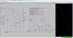
The curvature is at higher gate voltages deviates from the square law, or rather the curve "unbends". The best thing is to measure two points close to the actual circuit operating point. At least then the bias and transconductance estimates will come out right.
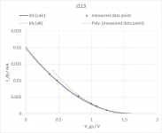
for 30 ohms and 47.5 ohms, V_gs0 1.73, I_dss 19.1
for 150 ohms and 330 ohms, V_gs0 1.60, I_dss 21.3
for 475 ohms and 1200 ohms, V_gs0 1.55, I_dss 24.0
for 30 ohms and 1200 ohms, V_gs0 1.59, I_dss 20.0
Note that my earlier estimate (where I used 250 and 330 ohms) worked out to very close to the value using expanded range of 30 and 1200 ohms (blue line), but that the values derived from the 475/1200 ohm pair (green dotted line) would give a better estimate for operating the circuit at R_s 1k.
Attachments
Last edited:
correction
**Note that my earlier estimate (where I used 150 and 330 ohms)**
And while I'm here: to clarify a point, since I can see this coming up-
It is no use obtaining the I_dss and V_gs0 values exactly if the intermediate current-voltage relationship cannot be predicted from these values, i.e. if the transfer function does not follow the square law: I_ds = I_dss (1-V_gs/V_gs0)^2
What we want instead is (arbitrary) I_dss and V_gs0 values which give usefully accurate predictions of DC operation and transconductance in the region of interest when used with the formula above and its derivations.
In that sense, a rule-of-thumb for the match measurement resistors can be stated as R1= R_s / 2 and R2 = R_s *2, where R_s is the source bias resistor in the actual circuit.
For around 1k source resistance, typical J113 characteristic is V_gs0 1.5 V and beta 9 mA/V^2. Within a range of V_gs0 1.3~1.7 the beta - and circuit values -don't change very much.
By making the bypass switchable partial/full, the circuit gain can be easily set to 36 dB and 56 dB so both MM and MC cartridges can be used without changing any resistors or capacitors or circuit currents. (for input loads, make your own daughterboard with dip switches etc ...)
I think this is a significant embellishment of the original concept, though it is only a convenience feature. The switch could be implemented on the boards with a 3-pin header jumper.
Attachments

Last edited:
Updated BOM, version 1.3c3.
No material changes to the circuit or parts, but I updated the worksheets to calculate the circuit gain for both MM and MC versions, and edited the annotation for clarity.
Only the drain resistors R2,8 vary with the JFET parameters, and when all is said and done the value can be simply tied to the JFET cut off voltage V_gs0 as follows,
V_gs0=1.3V~1.4V R2,8 = 22k
V_gs0=1.4V~1.5V R2,8 = 20k
V_gs0=1.5V~1.6V R2,8 = 18k
JFETs above 1.6V generate less voltage gain in the circuit and are best used for the followers Q2,4.
Attachments
Just the BOM this time, c4 revision.
The value of "beta" was incorrectly calculated in worksheet 1. This was for display only and did not affect results. It was correct in worksheet 2.
I removed all references to jfet "size" as it made things needlessly complicated. J113 can be classed by pinch-off voltage, V_gs0, and the drain resistors R2,8 can be chosen based on this parameter. It is made straightforward by the fact that the spread in beta is so small.
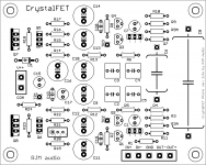
On a practical note, I have ordered some rev. 1.3c boards from pcbway and expect them late next week.
The value of "beta" was incorrectly calculated in worksheet 1. This was for display only and did not affect results. It was correct in worksheet 2.
I removed all references to jfet "size" as it made things needlessly complicated. J113 can be classed by pinch-off voltage, V_gs0, and the drain resistors R2,8 can be chosen based on this parameter. It is made straightforward by the fact that the spread in beta is so small.
On a practical note, I have ordered some rev. 1.3c boards from pcbway and expect them late next week.
Attachments
rev 1.2a board arrived today.
They are green. And they are not rev. 1.3c which will arrive later this week. And they'll only work as an mc phono stage at 56 dB or so.
So I am going to give them away. $5 for a set of two to cover postage&paypal. I have 10 sets. J113 JFETS supplied on request, $10 for a set of 2 matched pairs and 4 unmatched.
I think this is an excellent phono stage. I've been listening to mine break in over the last few days, both with headphones and traditional amp/speakers. It pretty much neutrally reproduces the source signal, but organically with no trace of grit, glare, or grain. Not the last word in bass slam or sizzle, but still properly extended to high and low frequencies. A gentle-sounding phono stage, if you will. Very easy to listen to.
Attachments

The rev 1.2a can be configed as mc with 56db gain and mm by left some capacitor out, right? I'll take a pair please.
RJM you evil I was deciding on your phonoclone for my turntable and start looking at what quality parts to get. Now you are tearing me apart with another piece of creation
interested to take a pair with matched Jfet, Any other way to pay you instead paypal me ?
interested to take a pair with matched Jfet, Any other way to pay you instead paypal me ?
Last edited:
As I wrote earlier, I prefer this JFET circuit to the phonoclone. It reminds me of both my early 6DJ8 passive RIAA stage and my Dad's Classe DR4 (phono stage uncoincidentally also made up of simple amplifier-follower stages, though with BJT for the amplifier)
Outside of Paypal, payment would have to take the form of a simple trade for RCA jacks other small parts. Or chocolate. I can do chocolate.
Outside of Paypal, payment would have to take the form of a simple trade for RCA jacks other small parts. Or chocolate. I can do chocolate.
Outside of Paypal, payment would have to take the form of a simple trade for RCA jacks other small parts. Or chocolate. I can do chocolate.
Sorry about my bad english, I mean do you have another paypal account ? currently in my region paypal hong kong, does not support paypal.me.
https://i.imgsafe.org/874f297.jpg.
An externally hosted image should be here but it was not working when we last tested it.
Last edited:
If paypal.me isn't available if your country you can send me your email address and I'll send you an invoice.
I can't accept money payments outside of Paypal, but as I noted above small trades are acceptable.
I can't accept money payments outside of Paypal, but as I noted above small trades are acceptable.
- Status
- Not open for further replies.
- Home
- Source & Line
- Analogue Source
- RJM Audio Crystal P jfet phono preamplifier | development thread