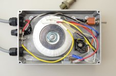
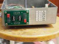
Today I switched out the power transfomer for a medical grade Triad VPM36-1390(50VA 2x18VAC).
They have both an electrostatic screen and a magnetic shield, and as an added bonus for me, the primary can be wired for the Japanese line voltage of 100 VAC.
I think these are tremendous value for money. Stocked at Digikey and Mouser.
I was having a bit of a problem in my home system with some buzzing in the speakers, relating to the phono stage but independent of preamp volume setting. I suppose leakage from the transformer was at fault as the VPM replacement is far, far quieter to the point of being inaudible. I was using the regular Triad previous to the upgrade.
Attachments
I really like the "apparent" simplicity of the design. Makes me feel better about my ignorance 🙂
And the thread has been really educational.
Thanks Richard
And the thread has been really educational.
Thanks Richard
Oh and as a true Pass fanboy, I couldn't resist seeing this as a variation of jboz-b1-riaa-jboz-b1, which probably tells much about how NP makes common design elements more user friendly, and connects them with his name at the same time.
And it's good to see experimentation with no unobtainium parts. But I still cannot help wondering how much of a difference would it make to optimize it for 2sk170.
It would be pretty easy to replace the buffer parts, just to see how much of a difference it would make both on the noise floor and on the sound.
Oh and I like the possibilities that your boards allow. They should be very nice for experimentation, playing around with variations of jboz and b1 style stages, replacing the riaa with a pot.
Last edited:
hey there, dimkasta, it's a been a while...
As you note, the follower (buffer) JFETs can be replaced with just about anything, but it's the amplifier stages that define the sound, in both noise and distortion.
The short story on the 2sk170 is I found them too expensive and too difficult to obtain in quantities large enough to bin and match. They will work though as the amplifier as per the many phono circuits kicking around the net using this device.
This looks like a great project. so the kit cost from your site covers all the boards and all components except for the box in the BOM for "additional parts"?
Vin
Vin
Last edited:
The kit is for boards, instructions, and all the parts that solder to the boards. Volume control, diodes, transformer, chassis, and chassis hardware are not included.
I've updated the BOM for this project. Shortened the JFET matching calculations so it's just one page instead of three sheets. The parts list is unchanged.
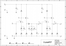
The long story here is that the JFET datasheet pinch off voltage (V_gs0) and saturation current (I_dss) parameters as you understand them are lies. The actual values you'd measure directly do not define the transfer characteristics of the transistor,
I = I_dss (1- V/V_gs0)^2 .
However, there is a set of constants, let's say A and B, that does define the JFET transfer curve quite well over a wide range of intermediate gate voltages, as
I = B (1- V/A)^2 .
Those constants of course "look" like V_gs0 and I_dss, but they aren't the same as the actual measured values.
The upshot of this is for the CrystalFET matching the "two measurement method" is correct and gives the optimal V_gs0 and I_dss values to simulate the device in the region of interest, derive the resistance R2,9 etc ... but these parameters will not be equal to the datasheet or measured values.
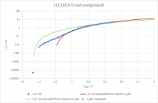
So, stick with the "two measurement method" and you will be OK. Also if you have an Atlas DCA75 Pro (I got one recently) it's also relatively easy to work out same parameters from the measured data. See me for details.
Finally, although I personally use this circuit as my MC phono stage it is "easier" to do as a MM stage. For one there is enough degenerative feedback that matching JFETs is much less critical, and for another there is enough gain to easily get about 35-36 dB. As an MC stage 53 dB seems to be about the maximum obtainable, and that's with "choice" transistors with the best balance of characteristics.
The long story here is that the JFET datasheet pinch off voltage (V_gs0) and saturation current (I_dss) parameters as you understand them are lies. The actual values you'd measure directly do not define the transfer characteristics of the transistor,
I = I_dss (1- V/V_gs0)^2 .
However, there is a set of constants, let's say A and B, that does define the JFET transfer curve quite well over a wide range of intermediate gate voltages, as
I = B (1- V/A)^2 .
Those constants of course "look" like V_gs0 and I_dss, but they aren't the same as the actual measured values.
The upshot of this is for the CrystalFET matching the "two measurement method" is correct and gives the optimal V_gs0 and I_dss values to simulate the device in the region of interest, derive the resistance R2,9 etc ... but these parameters will not be equal to the datasheet or measured values.
So, stick with the "two measurement method" and you will be OK. Also if you have an Atlas DCA75 Pro (I got one recently) it's also relatively easy to work out same parameters from the measured data. See me for details.
Finally, although I personally use this circuit as my MC phono stage it is "easier" to do as a MM stage. For one there is enough degenerative feedback that matching JFETs is much less critical, and for another there is enough gain to easily get about 35-36 dB. As an MC stage 53 dB seems to be about the maximum obtainable, and that's with "choice" transistors with the best balance of characteristics.
Attachments
Last edited:
Re-reading that last post perhaps an explainer is in order:
Originally I came up with the two measurement method (derivation of V_gs0 and I_dss from two sets of V_gs, I_ds data points) as a way to obtain those values if you didn't have a way to measure them directly. I was confused because my method did not result in values that agreed with datasheet or direct measurement.
Now I understand that in terms of modelling how the FET will behave in the circuit, the measured/datasheet V_gs0 and I_dss values are not very helpful, while the incorrect/optimized/nominal V_gs0 and I_dss derived from measured data points along the transfer curve do actually serve as good reference parameters for the calculations.
So the two measurement method is promoted from a curiosity and alternative method to really the best way to match and model JFETs in the CrystalFET.
Either two pairs if (I,V) measurements are needed, preferably close to the operating point of the JFET in the circuit, or, alternatively, one current measurement (I,V) and one transconductance measurement (dI/dV,V).
Changing the source resistor gives two (I_ds, V_gs) pairs, while something like the Atlas DCA75 will give you the gate voltage at 5 mA and the average transconductance between 3-5 mA, gfs. To obtain the transconductance at 5 mA, multiply the value by sqrt(5/4) ~ 1.1.
BOM 14e3
Added some notes regarding JFET matching. If you have a DCA75 you can match JFETs to the Vgs measured at 5 mA. Devices with Vgs = -0.5~-0.7 V are viable for Q1,3. Larger Vgs devices can be used for Q2,4. Use R2,9 = 22k.
Outside of the fuss of JFET matching my main concern with this circuit is gain. With the MC switch the JFETS are running maxed out and I estimate the gain is only about 52-53 dB. With this setup the MM gain ends up about 35 dB.
From a design standpoint the CrystalFET works a lot better as a dedicated MM stage, since the degenerative feedback used to reduce the gain not only improves distortion performance and reduces the required tolerances for matching devices, it also means the gain can be freely adjusted.
If you want to give up MC use and optimize the CrystalFET as an MM only phono stage with 40 dB of gain, reduce R4 and R11 to 150 ohms and R2 and R9 to 15 kohms. Not only is the gain increased but the FETs now run at higher current which improves performance slightly. The MC gain obtained in this configuration will be too low to be useable however, about 46 dB, so this mod means MM only operation essentially.
Attachments
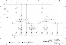
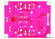
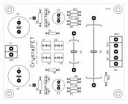
CrystalFET Rev. 2.0c
My intuition tells me this is the version of the CrystalFET most of you wanted.
The voltage regulator and MM/MC switch are gone, this is strictly bring-your-own-power-supply and MM only (though it will work as MC with different values). Big capacitors and plenty of space. 38 dB gain typical. Relaxed tolerances for FET matching.
Attachments
2.0f with BOM
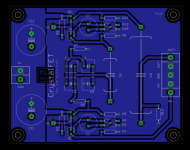
Easy job, since it was just taking a scalpel to the old 1.4 layout and then spreading everything that was left over out neatly over the board area.
Easy job, since it was just taking a scalpel to the old 1.4 layout and then spreading everything that was left over out neatly over the board area.
Attachments
doubling j113 at input?
Hi Richard,
I've studied the over long thread of the Salas folded phone pre which is very similar in topology as your creation (and is supposed to sound very nice).
But ... your creation is much easier to build as it is rather easy to source all the components (both jfets as well as riaa caps). My compliments for creating something that is practical to build!
I decided to build yours. Point-to-point as I always do.
There is one thing I wonder. Would it be beneficial to double the input jfet as in this schematic: https://www.diyaudio.com/forums/analogue-source/129126-simplistic-njfet-riaa-280.html#post2018041
As I understand, doubling up the input jfets will lower noise at the cost of a higher input capacitance.
Is it worth a try in your circuit? Should I change any of the resistor values when doing so?
Thanks, MArco
> The short story on the 2sk170 is I found them too expensive and too difficult to obtain in quantities large enough to bin and match.
For what it's worth, you can make up a 2SK170BL equivalent from 2x 2SK209GR (matched) in parallel.
They are pretty much identical in terms of noise, transconductance, capacitances, ...., etc.
And the 2SK209GR is < 0.5USD a pice at Digikey.
More info on still active N-JFETs can be found :
NJFETs for Source Follower Applications
Measurements Rate SMT Low-Voltage n-JFETs Under Consistent Conditions | Electronic Design
https://www.diyaudio.com/forums/pass-labs/175040-fet-noise-measurements-euvl-7.html#post5607021
Still plenty of choices with close to 2SK170 performance.
Cheers,
Patrick
What would you consider to be the best substitute for the 2SK170, other than the Linear Systems LSK170 which is supposed to be an identical replacement for the original?
Last edited:
2x 2SK209GR in parallel.
You can also use 1x 2SK2145GR and wire it in parallel.
Has to be GR grade.
I trust Toshiba.
I know what resources they have in their process development.
Patrick
You can also use 1x 2SK2145GR and wire it in parallel.
Has to be GR grade.
I trust Toshiba.
I know what resources they have in their process development.
Patrick
Forgot to mention that 2SK209 is of course the SMD version of 2SK117.
And 2SK117 should be still available at reasonable cost :
www.segor.de/#?Q=$:3876
2SK117-GR
LOT of 50 2SK117-GR , Transistor JFET Low Noise , N-CH Si 3-Pin, TO-92 | eBay
Patrick
And 2SK117 should be still available at reasonable cost :
www.segor.de/#?Q=$:3876
2SK117-GR
LOT of 50 2SK117-GR , Transistor JFET Low Noise , N-CH Si 3-Pin, TO-92 | eBay
Patrick
Nice to know that there are good alternatives to 2sk170 that are still available.
Still, I like Richards version also for the RIAA cap values. So it might still be a good idea to double up (or even quadruple) on Q1 (the input jfet) to get higher gain and/ or lower noise.
I've not a clue of how to calculate the source and load resistors in such case. May I just use the spreadsheet provided and double the Idss?
- Status
- Not open for further replies.
- Home
- Source & Line
- Analogue Source
- RJM Audio Crystal P jfet phono preamplifier | development thread